
Real-Time Dynamics Se

May 21, 2025 – A collaborative team from the University of Nottingham (UK), the SuperSTEM Laboratory in Daresbury (UK) and Ulm University (Germany) reports a controllable route to in‑situ nano‑engineering of elemental selenium. By confining Se inside boron nitride and carbon nanotubes and manipulating the filler with a low‑voltage electron beam, the scientists created one‑dimensional phases with optoelectronic properties that can be tuned on demand. This three‑in‑one use of the electron beam – as imaging probe, spectroscopic tool and nanoscale press – opens a pathway toward designer semiconductors for flexible nanoelectronics.
Historically, selenium has played a pivotal role in solid-state physics1. Experiments performed on Se in the 1870s led to the discovery of photoconductivity2, the realization of the photovoltaic effect in solid semiconductors3, and its use as the photoactive component of the first solar cells4. Extensive research has since focused on producing and optimizing selenium-based semiconductors with defined allotropes, driven by the phase- and dimensionality-dependent nature of their electronic and optical properties5,6.
The cylindrical inner cavities of carbon nanotubes (CNTs) provide confined reaction environments for the templated growth of high aspect ratio nanomaterials and enable atomically resolved studies of such structures using transmission electron microscopy (TEM)7,8. This approach has been applied to diverse semiconducting materials including SnSe9 and CsPbBr310, as well as to the elemental chalcogens sulfur11, selenium12, and tellurium13.
Selenium has been placed inside CNTs of many diameters before, and boron nitride nanotubes (BNNTs) have recently emerged as an attractive alternative host.
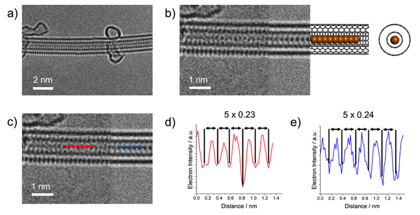
Aberration-corrected transmission electron microscopy (AC-TEM), supported by image simulations, was employed to investigate how the internal diameter of CNTs affects the structure and bonding of encapsulated selenium nanowires (Se NWs). The narrowest CNT studied (Fig. 1), with an inner diameter of 0.73 nm, hosts a linear atomic chain of selenium (l-Se), whose structure is shown in Fig. 1b. TEM simulations for l-Se within a CNT of matching diameter closely reproduce the experimental observations, revealing interatomic distances of 0.23 nm in the image and 0.24 nm in the model. The longest uninterrupted l-Se chain identified by AC-TEM spans at least 28 nm (Fig. 1a).
While previous Raman spectroscopic studies suggested the formation of l-Se chains within cancrinite nanochannels20, direct imaging evidence had been lacking. The structure observed here for l-Se under extreme confinement is consistent with findings on other chalcogens: both sulfur11 and tellurium13 have been shown to adopt linear chain configurations in narrow nanotube environments.
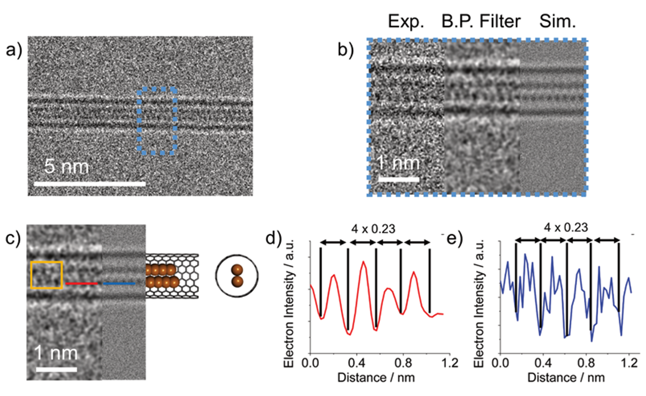
Additionally, the atomic spacing of selenium along the linear chains was measured as 0.23 nm in both experimental and simulated images (Fig. 2). As illustrated by the yellow square in Fig. 2c, two co-linear Se chains exhibit a staggered arrangement, likely resulting from the optimization of van der Waals interactions between adjacent atoms.
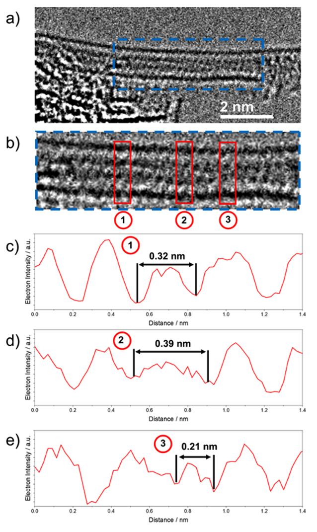
In some instances, the two co-linear l-Se chains were observed to twist along the axis of the CNT (Fig. 3), producing variations in their projected inter-chain distances. Similar co-linear atomic arrangements have previously been reported for tellurium encapsulated in 1.2 nm CNTs by Qin et al.21 The co-linear Se chains observed here may exhibit similar dynamic behavior to the double helices described by Fujimori et al.12, where rapid motion impeded atomic resolution imaging. In contrast, the present study focuses on stationary chain configurations, enabling precise determination of selenium atomic positions.
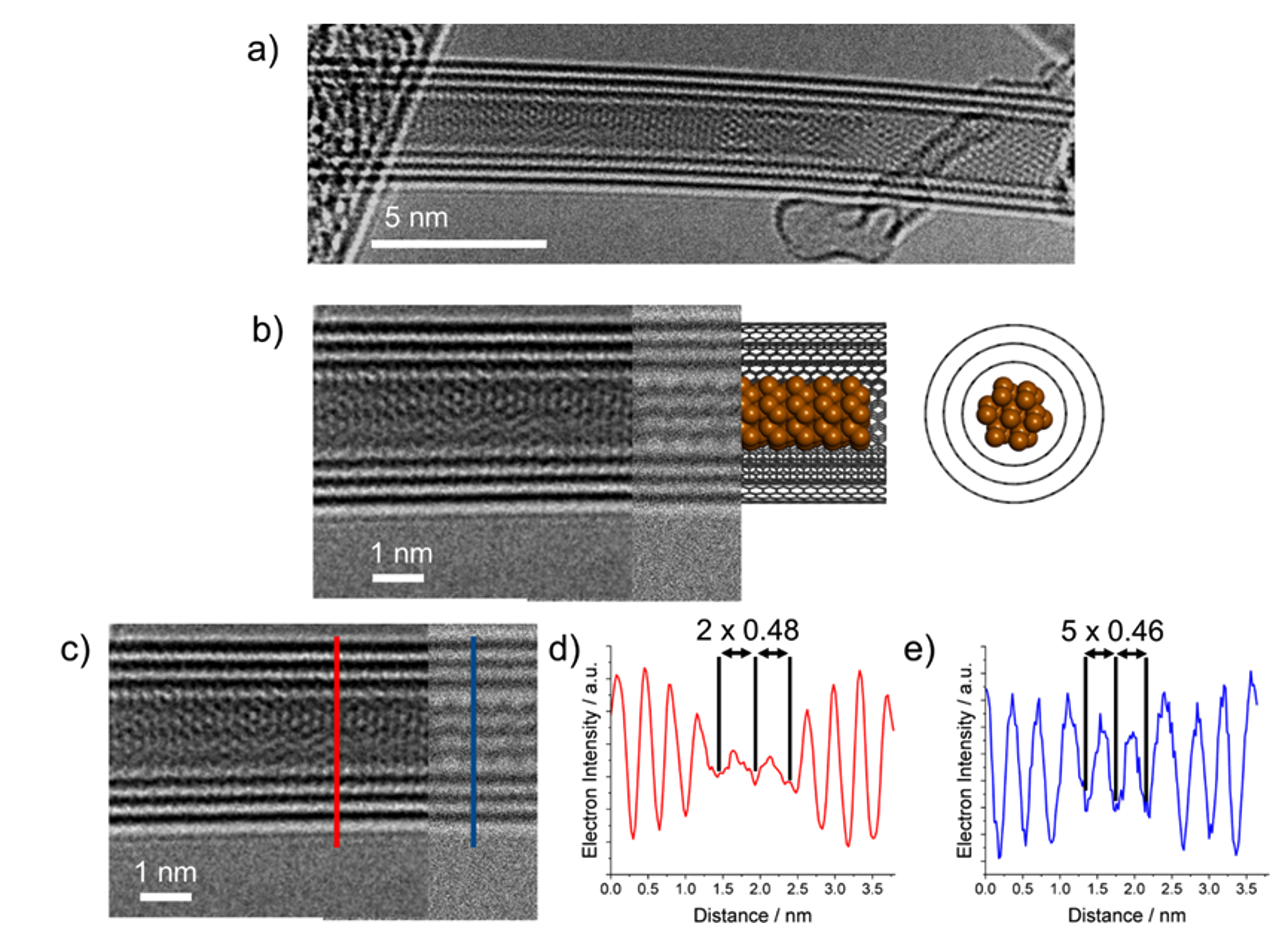
Due to van der Waals constraints, the maximum selenium-based structure that can be encapsulated in narrow CNTs consists of two t-Se chains. The internal diameter of the CNT governs the separation between these chains by mediating favorable interactions with the CNT walls22, resulting in increased inter-chain spacing as the CNT diameter increases. Larger diameters allow for the encapsulation of multiple t-Se chains (Fig. 4), as verified by matching simulated and experimental images. Together, these observations yield a one-dimensional phase diagram that predicts the structure of the selenium from the inner diameter of the host tube, whether CNT or BNNT: a single linear chain at 0.73 nm, t-Se chains in slightly wider tubes, several parallel chains in wider ones, and liquid-like selenium with menisci above about 3 nm.
Even in wider CNTs the encapsulated Se nanowires stay highly mobile: they lose long-range order but keep the short-range order of crystalline selenium.
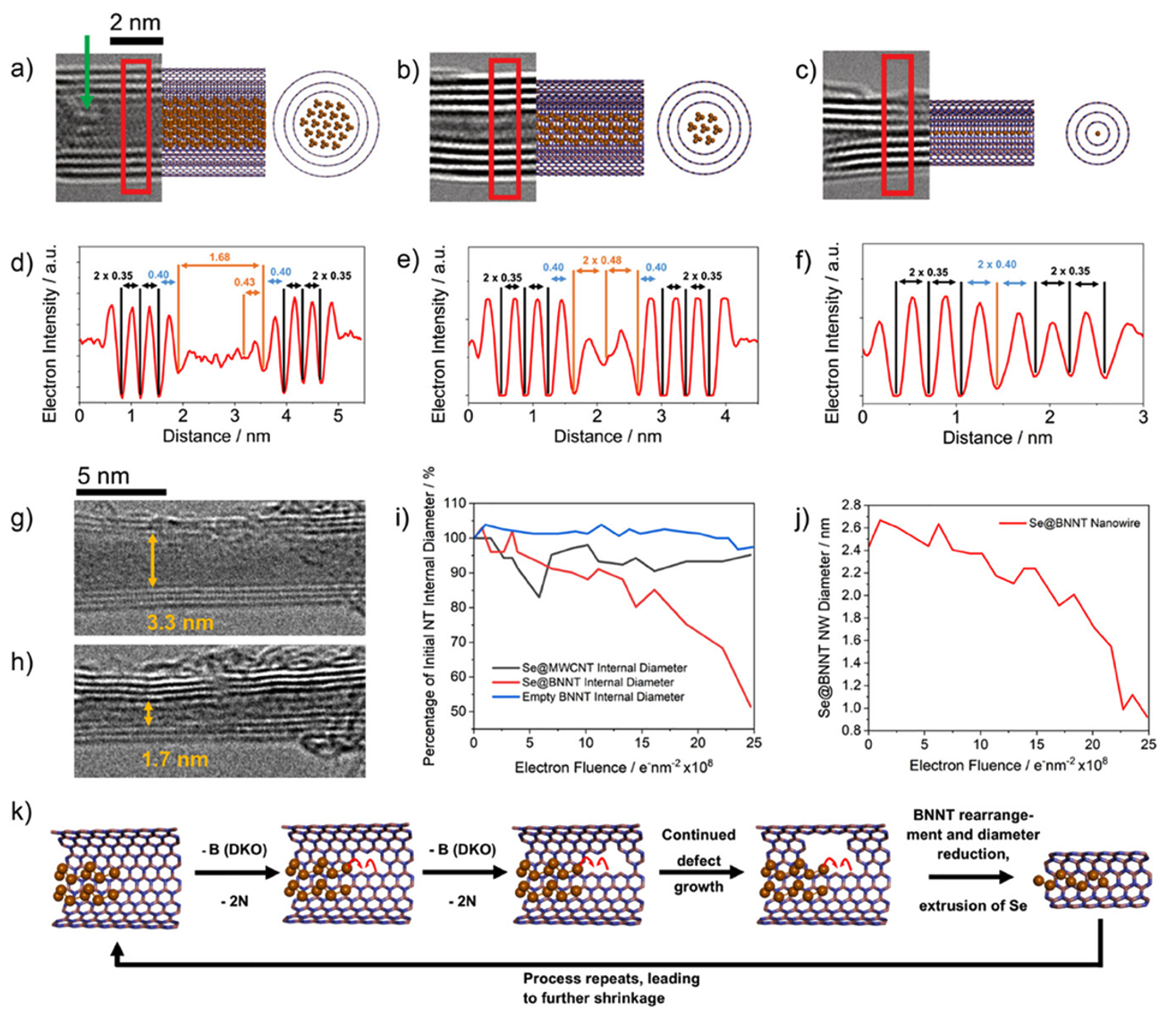
To further investigate the electron-beam-induced transformations, Se-filled BNNTs (Se@BNNT) were imaged under 80 kV AC-HRTEM at a controlled electron flux of 1.2 × 10⁸ e−nm−2 s−1. During irradiation, single BNNTs showed the formation of sidewall defects (green arrow, Fig. 5a), which progressively expanded due to direct knock-on (DKO) damage. As previously demonstrated for empty BNNTs by Celik-Aktas et al.26 and Cheng et al.27, the removal of boron atoms can also destabilize neighboring nitrogen atoms, resulting in mass loss from the irradiated nanotube.
This phenomenon progresses faster in inner walls of multi-walled BNNTs due to their higher curvature and strain26,27. Prolonged imaging (400 s) revealed lines of contrast interpreted as chains of Se forming near BNNT sidewall defects (Fig. 5a). As this contrast proved reversible, it was attributed to a temporary suppression of translational and rotational motion of the encapsulated t-Se, rather than a permanent crystalline phase transformation.
Importantly, the authors observed that vacancy defects in BNNTs not only propagated but also restructured under continuous electron beam exposure, causing the BNNT diameter to shrink. This behavior mirrors the annealing and structural reorganization processes previously observed26,27. Here, the diameter contraction of BNNTs directly induces a phase transition from t-Se to l-Se in the encapsulated material.
A comparable beam-induced extrusion process has been reported for carbon nanotubes in Fe@MWCNT systems, although it required simultaneous heating to 600 °C28. As the BNNT diameter narrowed under irradiation, increasingly confined Se NWs formed, showing characteristic t-Se interchain distances consistent with those in narrow CNTs. Eventually, single linear Se chains (Fig. 5c,f) were observed in BNNTs with inner diameters as small as 0.8 nm, consistent with the 1D phase diagram derived from CNT-based systems.
The structural motifs—linear chains (Fig. 5c), seven t-Se chains (Fig. 5b), and smeared contrast in wide nanotubes (Fig. 5h)—mirror those found in CNTs. Although selenium interacts more strongly with BNNT walls22, these interactions are insufficient to prevent the mobility of the encapsulated chains. The authors expect the narrowed BNNTs formed during irradiation to be structurally stable26,27, suggesting that the Se nanowires templated under these dynamic conditions may resemble those observed in CNTs at ambient conditions.
Selenium itself most likely speeds up this shrinkage by bonding to the dangling bonds at the vacancies, an effect not seen in CNTs.
The band gaps of the confined nanowires were measured with ultra-low-loss electron energy-loss spectroscopy (EELS), for which BNNTs are the better host: unlike CNTs, they do not mask the signal of the filling.
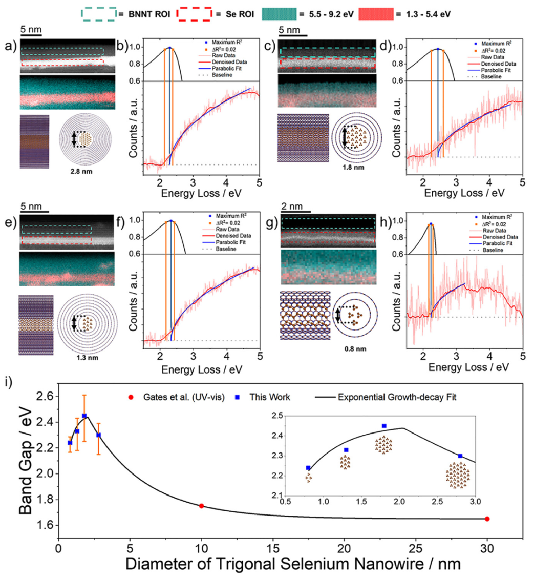
To prevent knock-on damage during data acquisition, high-angle annular dark-field (HAADF) AC-STEM imaging (Fig. 6a,c,e,g) and corresponding AC-STEM–EELS analysis (Fig. 6b,d,f,h) were conducted at an acceleration voltage of 60 kV. The internal diameters of the filled BNNTs studied exceeded 1.4 nm, a range which—according to the 1D Se phase diagram—favors the formation of nanowires (NWs) with similar crystalline disorder but differing in diameter.
EELS analysis revealed a maximum bandgap of 2.45 eV in a 1.8 nm diameter BNNT, where the encapsulated t-Se NW consists of approximately 20 helical chains (Fig. 6c,i, inset). This widening of the bandgap is attributed to quantum confinement effects33.
Interestingly, as the BNNT diameter was reduced from 1.8 nm to 0.8 nm, the observed bandgap narrowed to 2.24 eV, corresponding to a structure containing only four t-Se helices (Fig. 6g,i, inset). This trend highlights the complex interplay between structural dimensionality and optical properties in confined selenium phases. The band gaps measured on single nanowires are consistent with the orange colour of the Se@BNNT powder.
In summary, recent studies by Qin et al.21 and Milligan et al.19 have demonstrated the successful integration of semiconductors encapsulated in boron nitride nanotubes (BNNTs) into field-effect transistors and optoelectronic nanodevices. These devices combine favorable form factors, chemical inertness, and high performance.
However, broader applicability hinges on the ability to understand and control the intrinsic properties of the confined semiconductors. The present study shows that the dimensions, atomic structures, and bandgaps of semiconducting nanowires within BNNTs can be modulated with precision using low-voltage aberration-corrected transmission electron microscopy (AC-TEM).
This control over key material characteristics paves the way for the targeted design and functionalization of future nanoscale electronic devices. The work also underscores the multifunctionality of the electron beam, which acts simultaneously as an imaging, spectroscopic, and nanofabrication tool—highlighting its central role in advanced nanomaterials research.
Resource:
Cull, W. J., Ramasse, Q. M., Biskupek, J., Rance, G. A., Cardillo-Zallo, I., Weare, B. L., Fay, M. W., Whitney, R. R., Scammell, L. R., Fernandes, J. A., Kaiser, U., Patanè, A., & Khlobystov, A. N. (2025).
Flexible Selenium Nanowires with Tuneable Electronic Bandgaps.
Advanced Materials, 2025, 2501821.
https://doi.org/10.1002/adma.202501821
 Download this news article as PDF – for reading on paper, taking notes or filing.
-
Cherin, P., & Unger, P. (1967). The crystal structure of trigonal selenium. Inorg. Chem., 6(8), 1589–1591. https://doi.org/10.1021/ic50054a037
-
Smith, W. (1873). The action of light on selenium. J. Soc. Telegraph Eng., 2, 31. https://doi.org/10.1049/jste-1.1873.0023
-
Adams, W. G., & Day, R. E. (1877). IX. The action of light on selenium. Phil. Trans. Roy. Soc. Lond., 167, 313–349. https://doi.org/10.1098/rstl.1877.0009
-
Fritts, C. E. (1883). ART. LII. – On a new form of selenium cell, and some electrical discoveries made by its use. Am. J. Sci., 26(156), 465. https://doi.org/10.2475/ajs.s3-26.156.465
-
Bisht, N., Phalswal, P., & Khanna, P. K. (2022). Selenium nanoparticles: A review on synthesis and biomedical applications. Mat. Adv., 3(3), 1415–1431. https://doi.org/10.1039/d1ma00639h
-
Al Jahdaly, B. A., Al-Radadi, N. S., Eldin, G. M., Almahri, A., Ahmed, M. K., Shoueir, K., & Janowska, I. (2021). Selenium nanoparticles synthesized using an eco-friendly method: dye decolorization from aqueous solutions, cell viability, antioxidant, and antibacterial effectiveness. J. Mater. Res. Technol., 11, 85–97. https://doi.org/10.1016/j.jmrt.2020.12.098
-
Skowron, S. T., Chamberlain, T. W., Biskupek, J., Kaiser, U., Besley, E., & Khlobystov, A. N. (2017). Chemical reactions of molecules promoted and simultaneously imaged by the electron beam in transmission electron microscopy. Acc. Chem. Res., 50(8), 1797–1807. https://doi.org/10.1021/acs.accounts.7b00078
-
Fung, K. L., Weare, B. L., Fay, M. W., Argent, S. P., & Khlobystov, A. N. (2023). Reactions of polyaromatic molecules in crystals under electron beam of the transmission electron microscope. Micron, 165, 103395. https://doi.org/10.1016/j.micron.2022.103395
-
Faulques, E., Kalashnyk, N., Slade, C. A., Sanchez, A. M., Sloan, J., & Ivanov, V. G. (2022). Vibrational and electronic structures of tin selenide nanowires confined inside carbon nanotubes. Synth. Met., 284, 116968. https://doi.org/10.1016/j.synthmet.2021.116968
-
Kashtiban, R. J., Patrick, C. E., Ramasse, Q., Walton, R. I., & Sloan, J. (2023). Picoperovskites: the smallest conceivable isolated halide perovskite structures formed within carbon nanotubes. Adv. Mat., 35(10), 2208575. https://doi.org/10.1002/adma.202208575
-
Fujimori, T., et al. (2013). Conducting linear chains of sulphur inside carbon nanotubes. Nat. Commun., 4(1), 2162. https://doi.org/10.1038/ncomms3162
-
Fujimori, T., dos Santos, R. B., Hayashi, T., Endo, M., Kaneko, K., & Tománek, D. (2013). Formation and properties of selenium double-helices inside double-wall carbon nanotubes: experiment and theory. ACS Nano, 7(6), 5607–5613. https://doi.org/10.1021/nn4019703
-
Medeiros, P. V., et al. (2017). Single-atom scale structural selectivity in Te nanowires encapsulated inside ultranarrow, single-walled carbon nanotubes. ACS Nano, 11(6), 6178–6185. https://doi.org/10.1021/acsnano.7b02225
-
Loiseau, A., & Pascard, H. (1996). Synthesis of long carbon nanotubes filled with Se, S, Sb and Ge by the arc method. Chem. Phys. Lett., 256(3), 246–252. https://doi.org/10.1016/0009-2614(96)00459-9
-
Dutta, D., Gope, S., Negi, D. S., Datta, R., Sood, A. K., & Bhattacharyya, A. J. (2016). Pressure-induced capillary encapsulation protocol for ultrahigh loading of sulfur and selenium inside carbon nanotubes: application as high performance cathode in Li–S/Se rechargeable batteries. J. Phys. Chem. C, 120(51), 29011–29022. https://doi.org/10.1021/acs.jpcc.6b11017
-
Kobayashi, K., & Yasuda, H. (2015). Structural transition of tellurium encapsulated in confined one-dimensional nanospaces depending on the diameter. Chem. Phys. Lett., 634, 60–65. https://doi.org/10.1016/j.cplett.2015.05.047
-
Allard, C., et al. (2020). Confinement of dyes inside boron nitride nanotubes: photostable and shifted fluorescence down to the near infrared. Adv. Mat., 32(29), 2001429. https://doi.org/10.1002/adma.202001429
-
van Bezouw, S., et al. (2018). Diameter-dependent optical absorption and excitation energy transfer from encapsulated dye molecules toward single-walled carbon nanotubes. ACS Nano, 12(7), 6881–6894. https://doi.org/10.1021/acsnano.8b02213
-
Milligan, G. M., Cordova, D. L. M., Yao, Z. F., Zhi, B. Y., Scammell, L. R., Aoki, T., & Arguilla, M. (2024). Encapsulation of crystalline and amorphous Sb2S3 within carbon and boron nitride nanotubes. Chem. Sci., 15(27), 10464–10476. https://doi.org/10.1039/d4sc01477d
-
Poborchii, V. V., Lindner, G. G., & Sato, M. (2002). Selenium dimers and linear chains in one-dimensional cancrinite nanochannels: Structure, dynamics, and optical properties. J. Chem. Phys., 116(6), 2609–2617. https://doi.org/10.1063/1.1434950
-
Qin, J. K., et al. (2020). Raman response and transport properties of tellurium atomic chains encapsulated in nanotubes. Nat. Electron., 3(3), 141–147. https://doi.org/10.1038/s41928-020-0365-4
-
Jishi, R. A., White, C. T., & Mintmire, J. W. (2000). Endohedral selenium chains in carbon, boron nitride, and BC2N nanotubes. J. Quantum Chem., 80(3), 480–485. https://doi.org/10.1002/1097-461x(2000)80:3<480::aid-qua18>3.0.co;2-6
-
Chang, Y., Huang, L., Zhou, Y., Wang, J., & Zhai, W. (2022). Controlled localized phase transition of selenium for color-selective photodetectors. ACS Appl. Mater. Interfaces, 14(4), 5624–5633. https://doi.org/10.1021/acsami.1c22909
-
Laude, L. D., & Fitton, B. (1972). Effects of crystalline disorder on the electronic structure of selenium and tellurium. J. Non-Cryst. Sol., 8, 971–977. https://doi.org/10.1016/0022-3093(72)90255-4
-
Dittrich, B. (2021). On modelling disordered crystal structures through restraints from molecule-in-cluster computations, and distinguishing static and dynamic disorder. IUCrJ, 8(2), 305–318. https://doi.org/10.1107/s2052252521000531
-
Celik-Aktas, A., Stubbins, J. F., & Zuo, J. M. (2007). Electron beam machining of nanometer-sized tips from multiwalled boron nitride nanotubes. J. Appl. Phys., 102(2), 024310. https://doi.org/10.1063/1.2757007
-
Cheng, G., Yao, S., Sang, X., Hao, B., Zhang, D., Yap, Y. K., & Zhu, Y. (2016). Evolution of irradiation‐induced vacancy defects in boron nitride nanotubes. Small, 12(6), 818–824. https://doi.org/10.1002/smll.201502440
-
Sun, L., Banhart, F., Krasheninnikov, A. V., Rodriguez-Manzo, J. A., Terrones, M., & Ajayan, P. M. (2006). Carbon nanotubes as high-pressure cylinders and nanoextruders. Science, 312(5777), 1199–1202. https://doi.org/10.1126/science.1124594
-
Cao, K., et al. (2018). Comparison of atomic scale dynamics for the middle and late transition metal nanocatalysts. Nat. Commun., 9(1), 3382. https://doi.org/10.1038/s41467-018-05831-z
-
Björkman, T., Gulans, A., Krasheninnikov, A. V., & Nieminen, R. M. (2012). Van der Waals bonding in layered compounds from advanced density-functional first-principles calculations. PRL, 108(23), 235502. https://doi.org/10.1103/physrevlett.108.235502
-
Rafferty, B., & Brown, L. M. (1998). Direct and indirect transitions in the region of the band gap using electron-energy-loss spectroscopy. Phys. Rev. B, 58(16), 10326–10337. https://doi.org/10.1103/physrevb.58.10326
-
Hage, F. S., & Ramasse, Q. M. (2016). The low-loss spectrum of individual carbon nanotubes revisited at high energy resolution in real and momentum space. Microsc. & Microanal., 22(S3), 966–967. https://doi.org/10.1017/s1431927616005675
-
Mohammad, N. S. (2014). Understanding quantum confinement in nanowires: basics, applications and possible laws. J. Phys. Condens. Matter, 26(42), 423202. https://doi.org/10.1088/0953-8984/26/42/423202