First SALVE Sympsium held at Ulm University

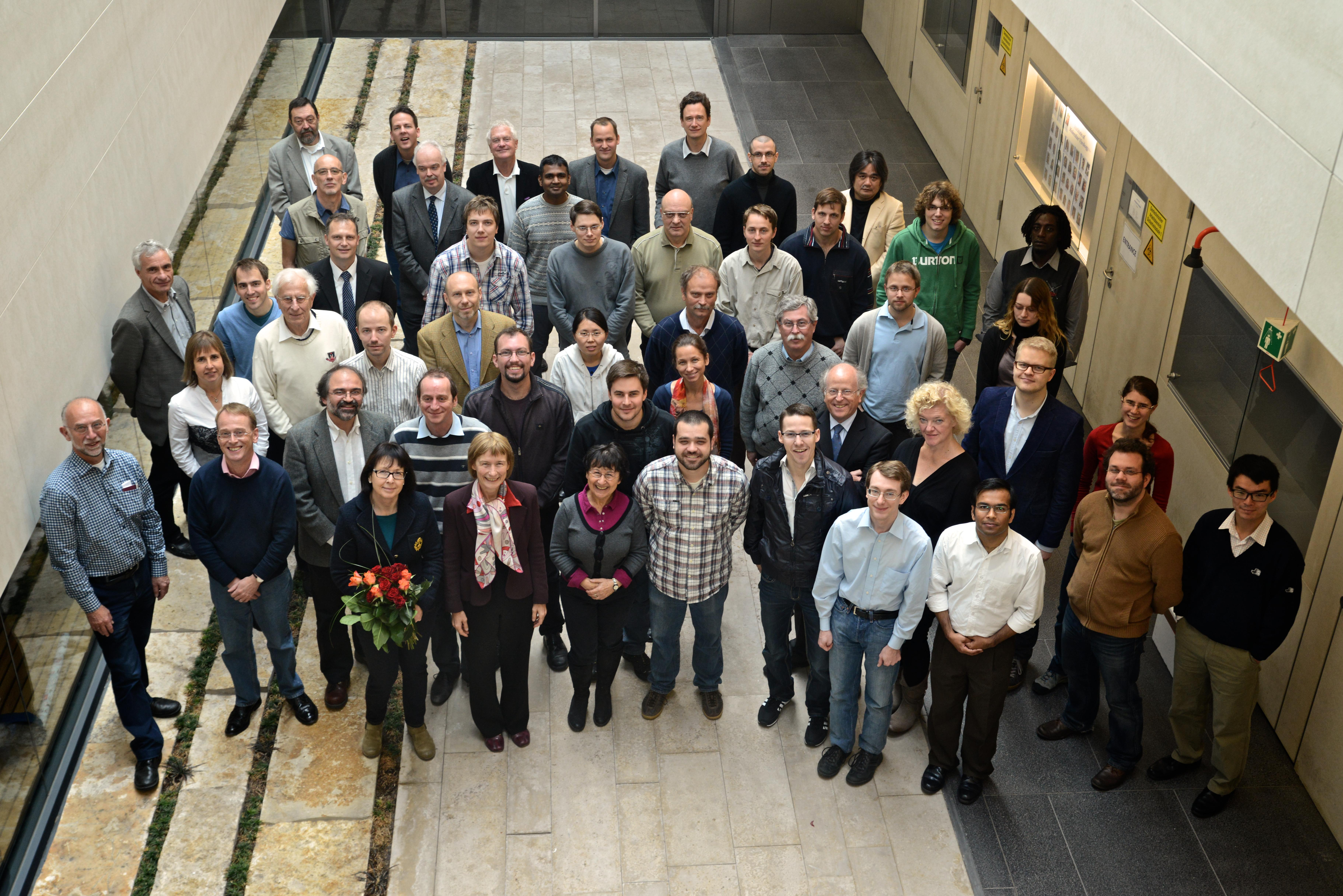
October 14-15, 2013 - More than 50 scientists (Fig. 1) met in Ulm, Germany, on the 15th of October 2013, for the international SALVE (Sub-Angstrom Low-Voltage Electron Microscopy) discussion meeting, following the physical colloquium and reception on the occasion of Ute Kaiser’s 60th birthday on the 14th of October, 2013. They shared one morning of intense discussions on current needs of low-voltage TEM for materials science and life science. The starting talks were given from Ulm University highlighted the progress that they have been achieved within the SALVE project with emphasis on instrumentation, imaging theory and application. The lively discussion resulted in a list of needs for developments in instrumentation and identified future topics in materials research that cannot be investigated using other techniques.
The discussion meeting attracted participants from 10 countries: Austria, Denmark, Finland, Germany, Hungary, Japan, the Netherlands, Sweden, the United Kingdom and the USA. The workshop was sponsored by the companies CEOS, FEI, and Zeiss.
The workshop was chaired by professor Ute A. Kaiser from Ulm University. In her welcoming words, Ute Kaiser reviewed the international trends on low voltage S/TEM.
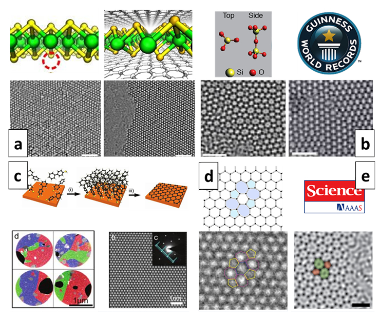
The Kaiser-Team at Ulm University presented their main results on instrumentation and application achieved in the SALVE-project. With the following figures we summarize main results of these talks:
Presentation of the Group of Electron Microscopy for Materials Science (EMMS)Physical Colloquium and Reception on the occasion of Ute Kaiser’s birthday (PDF):
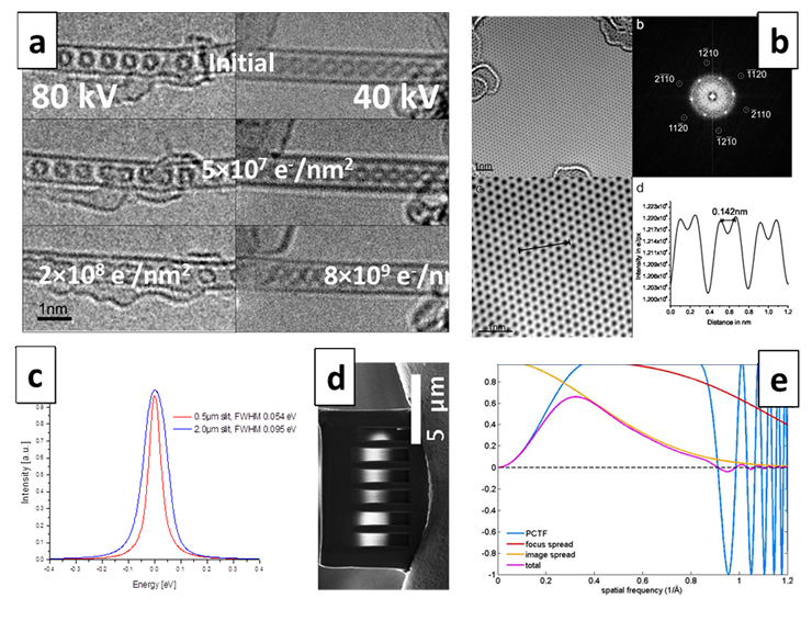
9:15 - 9:30 Johannes Biskupek The first talk on SALVE instrumentation including sample preparation emphasised the latest results obtained with the Cc/Cs corrected SALVE II instrument operated at 40kV. [1]
View graphical summary
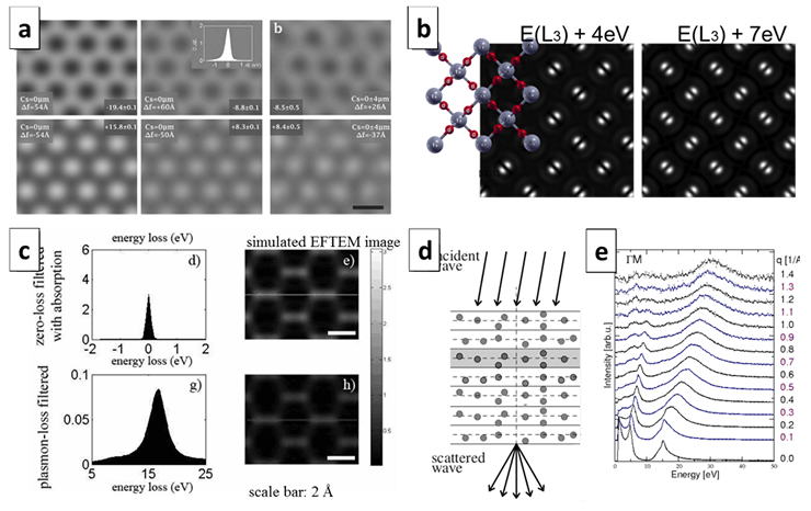
9:30 - 9:45 Ralf Hambach Inelastic scattering: Theory and experiments. [2 - 5]
View graphical summary
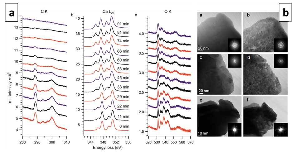
9:45 - 10:00 Ute Golla-Schindler In situ observation of electron beam-induced phase transformation of calcite as function of the accelerating voltage. [6]
View graphical summary
10:00 - 10:15 Ossi Lehtinen Graphene and other 2D materials in the TEM. [7 - 11]
View graphical summary
The talks were followed by a lively discussion session addressing the needs of low voltage electron microscopy. This summary presents the most important aspects of the discussion.
Current limitations of the Cc-corrector and the instrument in generalPeter Hartel (CEOS) explained that they have found the source for resolution limitations, which are the thermally moving electrons creating magnetic field and deviating the imaging electron. They showed that image spread depends on the square root of temperature, therefore He cooling not only of the objective lens but also the liner tube is advised; moreover increase metallic surroundings and beam paths nearer the optical axis should help. A short Cs corrector has no problems with the Jonson noise.
Ute Kaiser (Ulm University) said that we need to address all components in the surrounding of the objective. Smaller pole piece gap to reduce the Johnson effect are requested which need more flexible sample holder. Heny Zandbergen (Delft University) added that smaller sample holders with more flexibility are no problem for special holders, even to make it UHV compatible.
Matthias Rodewald (JEOL) explained that customized developments are always very welcome, but it is a matter of resources, whether they can be fulfilled. Usually only small changes can be expected from companies (although on the ARM series they provide an improved sample holder).
Angus Kirkland (Oxford University) emphasised that careful mechanical adjustment helps to improve the resolution; however very important for low kV is the mechanical stability of the instrument (including sample holder) and stable power supplies. He said that we may learn from the synchrotron community who always, when parameters are changed come into a feedback loop. It were important to know how the aberrations change with e.g. beam tilt. Peter Hartel stated that currently there is no feedback loop.
All agreed that UHV is an important next step in TEM development. Kazu Suenaga (AIST, Japan) and Jannik Meyer (Vienna University) mentioned that currently the NION machine has the best UHV, JEOL, so far has it in special cases.
Imaging TheoryAngus Kirkland and Ute Kaiser reported about the calculation showing that already at 30kV graphene is no weak phase object.
Heny Zandbergen (Delft University) and Jannik Meyer (Vienna University) stated that it may make sense to go to thicker samples for better SNR. And moreover, dynamical diffraction may help a lot but needs a better modeling.
Peter Schatttschneider (TU Vienna) mentioned that inelastic process looks like an incoherent source and dynamical scattering will take place. Moreover he pointed that atomic resolution is no important for low losses because of long interaction area. But it is very strongly peaked at the center! At high losses we are hunting now for bonding effects.
Michael Lehmann, Heny Zandbergen and Angus Kirkland pointed to the difficulty of the potentials determination. Atoms are still assumed to be spherical and an inversion process still not possible.
SamplesEva Olsson (Goteborg University) and Heny Zandbergen mentioned an important new class of materials for low voltages: polymer-based solar cells. It seems in general a good strategy to perform (in-situ) experiments with 300 kV for structure formation and 40 kV for imaging.
Rasmus Schröder (Heidelberg University) pointed to the effect of different low voltages on biological samples. At 40 kV much less voids. It is likely that different damaging channels in dependence of acceleration voltage do exist.
Sample PreparationHeny Zandbergen (Delft University) commented to the possibility of sample preparation with the He-Ion microscope. However a few He atoms stay in the sample and are blowing up the sample with He.
Lajos Toth (Budapest, Hungary) commented on the sandwich structure that also surface diffusion can be reduced and graphene can block the microscope "vacuum" from the sample.
Jannik Meyer pointed out that cooling down the sample results in collecting all the water molecules and finally the sample falls apart. If two layers of graphene are separated by a spacer then the lower graphene sheet is faster being eaten away; Molecules on graphene are attached to grain boundaries, damage depends on which side the graphene is located. Is there modification of the molecule in the sandwich structure?
-
Lechner, L., J. Biskupek, and U. A. Kaiser (2012) Improved Focused Ion Beam Target Preparation of (S)TEM Specimen - A Method for Obtaining Ultrathin Lamellae. Micros. Microanal., 18: 379-384, doi: 10.1017/S1431927611012499
-
Lee, Z., J. C. Meyer, H. H. Rose, and U. A. Kaiser (2012) Optimum HRTEM image contrast at 20kV and 80kV – exemplified by graphene. Ultramicroscopy, 112: 39-46, doi: 10.1016/j.ultramic.2011.10.009.
-
Löffler, S., V. Motsch, and P. Schattschneider (2013) A pure state decomposition approach of the mixed dynamic form factor for mapping atomic orbitals. Ultramicroscopy, 131: 39, doi: 10.1016/j.ultramic.2013.03.021.
-
Lee, Z., H. H. Rose, R. Hambach, P. Wachsmuth, and U. A. Kaiser (2013) The influence of inelastic scattering on EFTEM images - exemplified at 20kV for graphene and silicon. Ultramicroscopy, 132: 102-112, doi: 10.1016/j.ultramic.2013.05.020.
-
Wachsmuth, P., R. Hambach, M. K. Kinyanjui, M. Guzzo, G. Benner, and U. A. Kaiser (2013) High-energy collective electronic excitations in free-standing single-layer graphene. Phys. Rev. B, 88: 075433, doi: 10.1103/PhysRevB.88.075433.
-
Golla-Schindler, U., G. Algara-Siller, A. Orchowski, Y. Wu, T. Weil, and U. A. Kaiser (2012) First results of 20 kV EFTEM of core-shell QDS with an albumin-derived polypeptide surface coating on graphene. In EMC 2012 15th European Microscopy Congress, 16-21 September 2012, Manchester, United Kingdom, 2 pages. , Download PDF.
-
Algara-Siller, G., S. Kurasch, M. Sedighi, O. Lehtinen and U. A. Kaiser (2013) The pristine atomic structure of MoS2 monolayer protected from electron radiation damage by graphene. Appl. Phys. Lett., 103: 203107 , doi: 10.1063/1.4830036.
-
Huang, P. Y., S. Kurasch, A. Srivastava, V. Skakalova, J. Kotakoski, A. V. Krasheninnikov, R. Hovden, Q. Mao, J. C. Meyer, J. Smet, D. A. Muller, and U. A. Kaiser (2012) Direct Imaging of a Two-Dimensional Silica Glass on Graphene. Nano Lett., 12: 1081 , doi: 10.1021/nl204423x.
-
Matei, D. G., N.-E. Weber, S. Kurasch, S. Wundrack, M. Woszczyna, M. Grothe, T. Weimann, F. Ahlers, R. Stosch, U. A. Kaiser and A. Turchanin (2013) Functional Single-Layer Graphene Sheets from Aromatic Monolayers. Adv. Mater., 25: 4146-4151 , doi: 10.1002/adma.201300651
-
Kotakoski, J., J. C. Meyer, S. Kurasch, D. Santos-Cottin, U. A. Kaiser and A. Krasheninnikov (2011) Stone-Wales-type transformations in carbon nanostructures driven by electron irradiation. Phys. Rev. B, 83: 245420 , doi: 10.1103/PhysRevB.83.245420.
-
Huang, P. Y., S. Kurasch, J. S. Alden, A. Shekhawat, A. A. Alemi, P. L. McEuen, J. P. Sethna, U. A. Kaiser, D. A. Muller (2013) Imaging Atomic Rearrangements in Two-Dimensional Silica Glass: Watching Silica’s Dance. Science, 342: 6155. , doi: 10.1126/science.1242248.