Inside Carbon Nanotubes: SALVE TEM reveals Graphene Ribbons in the Subnanometer Range
January 01, 2021 - Graphene nanoribbons (GNRs) are extremely interesting for nanoscale electronics and devices. However, the growth of high-quality GNRs with well-defined widths is still remaining a challenge. Furthermore, the analysis of the electronic properties of GNRs has remained challenging. Scientists from the Sun Yat-sen University in China, the Universities of Vienna, Budapest and Ulm in Europe and the National Institute of Advanced Industrial Science and Technology in Japan could now synthesize well-defined sub-nanometer GNRs inside carbon nanotubes (CNTs) and measure their electronic properties.
Thanks to the unique electronic properties of graphene [1], it is possible to create a band gap by reducing the width of graphene bands into the sub-nanometer range. The size of the band gap increases with the decreasing width of the GNR [2]. Such structures have interesting applications for future electronic devices [3]. At present, most of the common stripes are of the armchair type. The edge of the ribbons consists of coaxial carbon pairs aligned parallel to the direction of the ribbon axis.
There are many possibilities to further change the properties of the GNR, [4] z. B. by changing their edges. In general, the carbons at the edge of the ribbons are saturated with hydrogen. But by selecting special molecules, by bandgap technology [5], or by constructing band heterojunctions [6] new unusual properties can be created. Recently, GNRs also became relevant for applications in photocatalytic hydrogen generation [7]. Hybrid structures of encapsulated bands and a semiconducting SWCNT with a different band gap can also be very interesting.
Filling and carrying out subsequent chemical reactions in single-walled carbon nanotubes (SWCNTs) is a promising technique for producing nanoscale materials [8]. The European-Asian team of scientists has now shown that this method can be used to produce GNRs with a precisely defined width in the sub-nanometer range. The width of the GNRs is depending on the diameter of the SWCNTs.
The growth of GNRs in SWCNTs was shown by first filling the SWCNTs with flat precursor molecules such as corones [9, 10] or other PAHs [11] and then transforming them at elevated temperature. Although these first results were very promising because of the overlapping electronic transitions of the carbon nanotubes themselves. In order to avoid this overlap, the otherwise flawless tubes had to be functionalized [12].
Aberration Corrected High Resolution Transmission Electron Microscopy (AC-HRTEM)
The aberration-corrected high-resolution electron microscope (AC-HRTEM) enables these interesting subnanometer-sized two-dimensional objects to be examined more closely. One can depict the CNT and also objects inside with atomic resolution. In addition, using electron diffraction, one can determine other properties such as stacking and tube chirality. The electron beam can also be used to transform the band structure over time, which makes further interesting investigations possible.
“The AC-HRTEM can also differentiate between flat and tubular structures within the CNT,” says Ute Kaiser, who heads low voltage transmission electron microscopy at Ulm University. "But how can one determine the exact atomic structure and especially the electronic properties of the GNR?"
The new study now focused on enabling a simple and scalable approach for the controlled growth of various well-defined graphene nanoribbons in the sub-nanometer range, including the quantification of their electronic and structural parameters. The time-dependent AC-HRTEM data were used to show that the observed species are flat objects that twist under the influence of the electron beam and cannot be identified as inner nanotubes. Raman scattering combined with first principle calculations and resonance excitation analysis was then used to identify the structure of GNR.
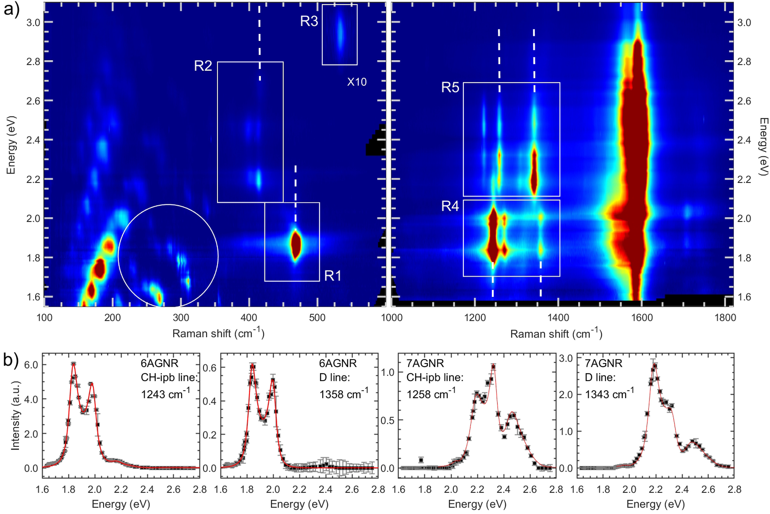
Examples for the TEM images are depicted in Figure 1 and for the Raman images in Box 1-3. Significant intensity difference can be observed between the edge of 7AGNR (Figure 1a) and the edge of the inner SWNT in DWNT (Figure 1e). Whereas for the nanoribbons@SWCNT the intensity profile for the inner objects is flat (Figure 1f, top), it exhibits strong maximum at the edge for the inner objects in SWCNT@SWCNT (Figure 1f, center and bottom).
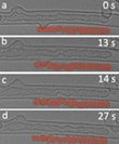
Next, the team explored the possibilities to determine the electronic properties of the GNR within CNT. The standard feature for the observation of encapsulated ribbons in TEM is an alternating pattern of narrow and wide signals from the material inside [11, 13]. It comes from twisting parts of the ligaments induced by electron beams. Figure 2 shows a collection of results from FeCp2-filled and subsequently transformed SWCNT species as recorded by the SALVE instrument with a Cs/Cc aberration corrector. It demonstrates the twisting of the graphene bands by the electron beam (panels a - e) and provides images of the bands in atomic resolution with corresponding simulations (panels f - j). The AC-HRTEM images (fields f - j) provide clear evidence of the atomic structure of the ribbons, but also show that the nanoribbons are very unstable under the electron beam and defects along the length of the structure are quickly created by the beam. Therefore, these AC-HRTEM images are not representative for the quality of the growing bands and only serve as evidence that the structures are flat bands. The instability of the TEM image with the irradiation time is shown in more detail in Figure 3.
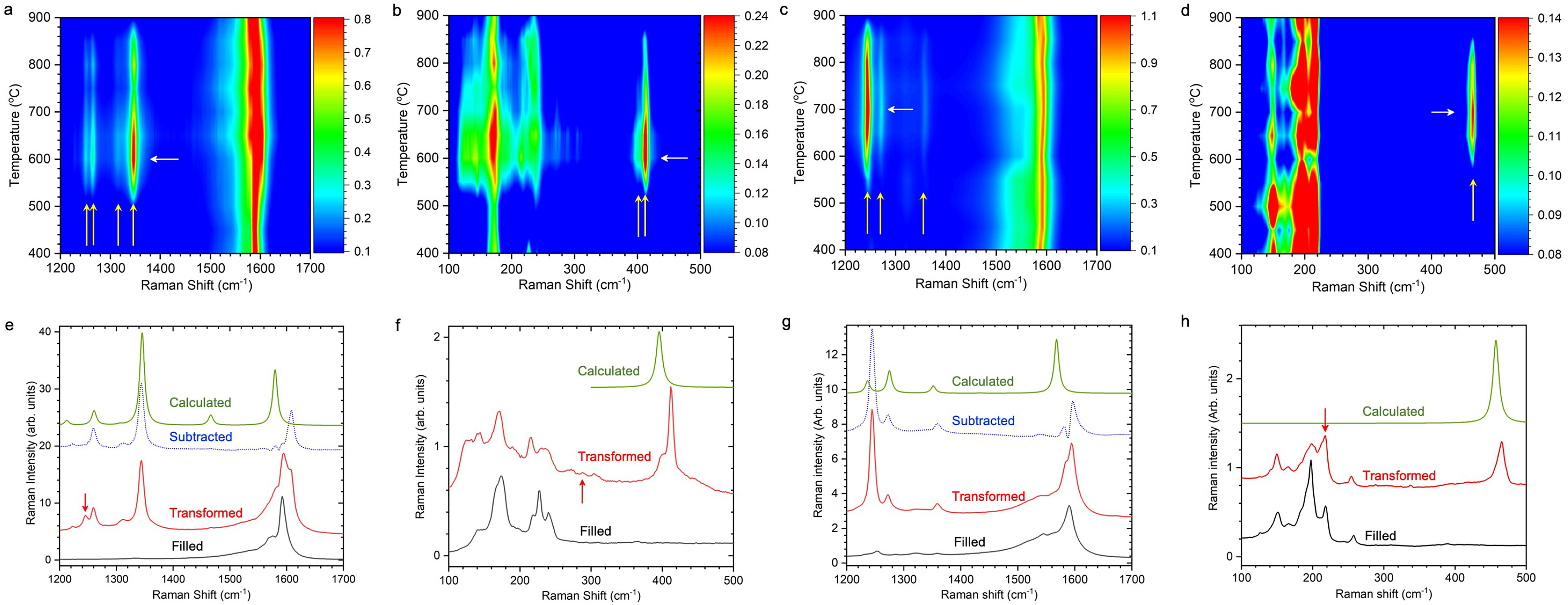
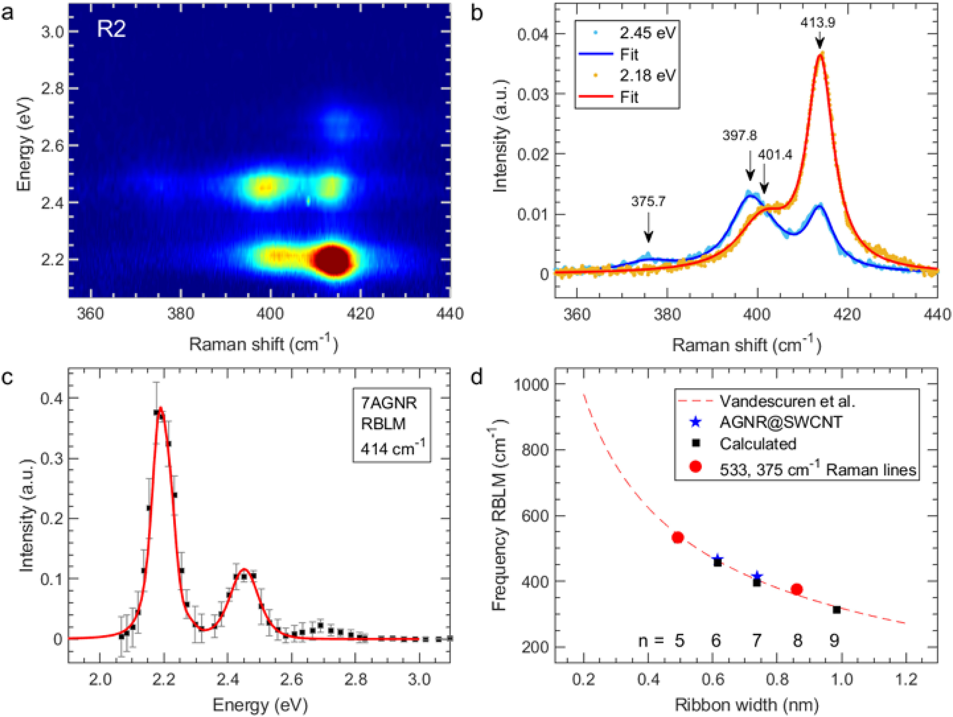
The authors of the study showed the synthesis of graphene nanoribbons with widths of 0.61 and 0.74 nm and excitonic gaps of 1.83 and 2.18 eV by high-temperature vacuum annealing of ferrocene molecules in single-walled carbon nanotubes. They obtained information the information on the precisely defined electronic structure of the growing ribbons from their detailed, wavelength-dependent Raman spectroscopic experiments. Raman scattering, especially the combination with the evaluation of resonance Raman excitation profiles, is an excellent tool for studying the electronic structure of the objects inside the tubes. This is due to the double selectivity of the resonance Raman scattering process. The Raman spectrum is selective with respect to the geometric structure of the GNR, but also selective with respect to its electronic structure. The narrow width of the Raman lines indicates well-defined geometrical structures, and sharp excitation profiles indicate a uniform electronic configuration of the GNRs. Thus, the Raman method enables the electronic structures of the bands to be determined.
The new study may be providing a solution to the long standing problem that bands with a larger or smaller width than those specified here can be grown in targeted SWCNTs and their structural and electronic properties can be studied with AC-HRTEM and Raman scattering thus open up a new field of subnanometer graphene nanoribbon research.
Resource: Kuzmany, H., Shi, L., Martinati, M., Cambré, S., Wenseleers, W., Kürti, J., Koltai, J., Kukucska, G., Cao, K., Kaiser, U., Saito, T. & Pichler, T. Well-defined sub-nanometer graphene ribbons synthesized inside carbon nanotubes. Carbon, 171, 221-229, 10.1016/j.carbon.2020.08.065, see also the supporting information.
-
Novoselov, K. S., Geim, A. K., Morozov, S. V., Jiang, D., Zhang, Y., Dubonos, S. V., Grigorieva, I. V., & Firsov, A. A. (2004). Electric field effect in atomically thin carbon films. Science, 306(5696), 666-669.
-
Son, Y. W., Cohen, M. L., & Louie, S. G. (2006). Energy gaps in graphene nanoribbons. Physical Review Letters, 97(21), 216803.
-
Bennett, P. B., Pedramrazi, Z., Madani, A., Chen, Y. C., de Oteyza, D. G., Chen, C., de Oteyza, D. G., Chen, C., Fischer, F. R., Crommie, M. F., & Bokor, J. (2013). Bottom-up graphene nanoribbon field-effect transistors. Applied Physics Letters, 103(25), 253114.
-
Gröning, O., Wang, S., Yao, X., Pignedoli, C. A., Barin, G. B., Daniels, C., Cupo, A., Meunier, V., Feng, X., Narita, A., Müllen, K., Ruffieux, P., & Fasel, R. (2018). Engineering of robust topological quantum phases in graphene nanoribbons. Nature, 560(7717), 209-213.
-
Verzhbitskiy, I. A., Corato, M. D., Ruini, A., Molinari, E., Narita, A., Hu, Y., Schwab, M. G., Bruna, M., Yoon, D., Milana, S., Feng, X., Müllen, K., Ferrari, A. C., Casiraghi, C., & Prezzi, D. (2016). Raman fingerprints of atomically precise graphene nanoribbons. Nano Letters, 16(6), 3442-3447.
-
Cao, T., Zhao, F., & Louie, S. G. (2017). Topological phases in graphene nanoribbons: junction states, spin centers, and quantum spin chains. Physical Review Letters, 119(7), 076401.
-
Akilimali, R., Selopal, G. S., Benetti, D., Mohammadnezhad, M., Zhao, H., Wang, Z. M., Stransfield, B., & Rosei, F. (2020). Graphene nanoribbon-TiO2-quantum dots hybrid photoanode to boost the performance of photoelectrochemical for hydrogen generation. Catalysis Today, 340, 161-169.
-
Khlobystov, A. N. (2011). Carbon nanotubes: from nano test tube to nano-reactor. ACS Nano, 5(12), 9306-9312.
-
Chernov, A. I., Fedotov, P. V., Talyzin, A. V., Suarez Lopez, I., Anoshkin, I. V., Nasibulin, A. G., Kauppinen, E. I., & Obraztsova, E. D. (2013). Optical properties of graphene nanoribbons encapsulated in single-walled carbon nanotubes. ACS Nano, 7(7), 6346-6353.
-
Anoshkin, I. V., Talyzin, A. V., Nasibulin, A. G., Krasheninnikov, A. V., Jiang, H., Nieminen, R. M., & Kauppinen, E. I. (2014). Coronene encapsulation in single‐walled carbon nanotubes: stacked columns, peapods, and nanoribbons. ChemPhysChem, 15(8), 1660-1665.
-
Chamberlain, T. W., Biskupek, J., Rance, G. A., Chuvilin, A., Alexander, T. J., Bichoutskaia, E., Kaiser, U., & Khlobystov, A. N. (2012). Size, structure, and helical twist of graphene nanoribbons controlled by confinement in carbon nanotubes. ACS Nano, 6(5), 3943-3953.
-
Lim, H. E., Miyata, Y., Fujihara, M., Okada, S., Liu, Z., Sato, K., Omachi, H., Kitaura, R., Irle, S., Suenaga, K., & Shinohara, H. (2015). Fabrication and optical probing of highly extended, ultrathin graphene nanoribbons in carbon nanotubes. ACS nano, 9(5), 5034-5040.
-
Chuvilin, A., Bichoutskaia, E., Gimenez-Lopez, M. C., Chamberlain, T. W., Rance, G. A., Kuganathan, N., Biskupek, J., Kaiser, U., & Khlobystov, A. N. (2011). Self-assembly of a sulphur-terminated graphene nanoribbon within a single-walled carbon nanotube. Nature Materials, 10(9), 687-692.
-
Kuzmany, H., Shi, L., Pichler, T., Kürti, J., Koltai, J., Hof, F., & Saito, T. (2015). The origin of nondispersive Raman lines in the D‐band region for ferrocene@ HiPco SWCNTs transformed at high temperatures. Physica Status Solidi (B), 252(11), 2530-2535.
-
Kuzmany, H., Shi, L., Kürti, J., Koltai, J., Chuvilin, A., Saito, T., & Pichler, T. (2017). The growth of new extended carbon nanophases from ferrocene inside single‐walled carbon nanotubes. Physica Status Solidi (RRL)–Rapid Research Letters, 11(8), 1700158.
-
Linck, M., Hartel, P., Uhlemann, S., Kahl, F., Müller, H., Zach, J., Haider, M., Niestadt, M., Bischoff, M., Biskupek, J., Lee, Z., Lehnert, T., Börrnert, F., Rose, H., & Kaiser, U. (2016). Chromatic aberration correction for atomic resolution TEM imaging from 20 to 80 kV. Physical Review Letters, 117(7), 076101.
-
Börrnert, F., & Kaiser, U. (2018). Chromatic-and geometric-aberration-corrected TEM imaging at 80 kV and 20 kV. Physical Review A, 98(2), 023861
-
Borin Barin, G., Fairbrother, A., Rotach, L., Bayle, M., Paillet, M., Liang, L., Meunier, V., Hauert, R., Dumslaff, T., Narita, A., Müllen, K., Sahabudeen, H., Berger, R., Feng, X., Fasel, R., & Ruffieux, P. (2019). Surface-synthesized graphene nanoribbons for room temperature switching devices: substrate transfer and ex situ characterization. ACS Applied Nano Materials, 2(4), 2184-2192.
-
Kuzmany, H., Imhoff, E. A., Fitchen, D. B., & Sarhangi, A. (1982). Frank-Condon approach for optical absorption and resonance Raman scattering in trans-polyacetylene. Physical Review B, 26(12), 7109.
-
Vandescuren, M., Hermet, P., Meunier, V., Henrard, L., & Lambin, P. (2008). Theoretical study of the vibrational edge modes in graphene nanoribbons. Physical Review B, 78(19), 195401.
-
Talirz, L., Ruffieux, P., & Fasel, R. (2016). On‐surface synthesis of atomically precise graphene nanoribbons. Advanced Materials, 28(29), 6222-6231.
-
Skowron, S. T. et al. Chemical reactions of molecules promoted and simultaneously imaged by the electron beam in transmission electron microscopy. Acc. Chem. Res. 50, 1797–1807 (2017).


