
Chemical Modification of 2D TMPTs

September 1, 2022 – Transition metal phosphorus trisulfides (TMPTs) are layered materials with intrinsic magnetic properties. Researchers from Ulm University, the Helmholtz-Zentrum Dresden-Rossendorf and Aalto University have analysed in detail how the electron beam (30–80 kV) of the aberration-corrected SALVE microscope interacts with few-layer MnPS3, FePS3 and NiPS3. Sulfur leaves first, oxygen moves in, and the defects add new states to the band gap, opening a way to tune ultrathin freestanding TMPTs by controlling their stoichiometry.
Some of the most intriguing magnets of the moment are only a few atoms thick. Two-dimensional (2D) materials already offer a wide range of fascinating electronic, optical and magnetic properties[1]–[4], and stacking individual layers creates heterostructures with properties of their own[5]–[7]. A promising family among them are the transition metal phosphorus trisulfides (TMPTs), layered compounds such as MnPS3, FePS3 and NiPS3[8],[9]. Their band gaps span a wide range[10], from 1.5 to 3.0 eV[11],[12], and they consist mostly of earth-abundant, non-toxic elements[13], which makes them candidates for optoelectronics[14]. Above all, TMPTs are intrinsically magnetic: they are among the most recently studied antiferromagnetic 2D materials[15],[16], because their magnetic order survives down to a few layers[17], so they can serve as test beds for the fundamentals of 2D magnetism[13],[18]. Their layered structure also invites intercalation of ions or molecules[19], which makes them interesting for energy storage[20]–[22]; because lithium binds strongly to their surface, TMPTs have even been predicted to work as anodes in lithium-ion batteries[23].
Early theoretical and experimental work showed that the properties of these materials can be tuned. Under high pressure, for example, MnPS3 and MnPSe3 undergo a cooperative spin crossover and a semiconductor-to-metal transition[24]. Defects, however, had hardly been studied experimentally, although calculations for single layers predicted striking defect-induced changes in the electronic and magnetic properties, such as spin-split states inside the band gap of MnPS3[25]. Several studies reported stacking faults in various TMPTs[26],[27] and showed that they strongly change properties such as the thermal conductivity[28], yet how defects act in few-layer systems remained open.
Transmission electron microscopy (TEM) is a particularly powerful tool here, because its fast electrons can modify[29],[30], probe[31]–[34] and individually address[35]–[39] the atoms of freestanding nanosheets. Aberration-corrected (AC) high-resolution TEM (HRTEM) correlates chemical and crystallographic information down to the atomic scale[40]–[42]. A prerequisite is clean, freestanding few-layer TMPT samples, which polymer-assisted mechanical exfoliation recently made possible[43]. What had been missing was a detailed study of how electrons in the low-voltage range of 30–80 kV, chosen to minimise damage[44], interact with these ultrathin crystals. A team from Ulm University, the Helmholtz-Zentrum Dresden-Rossendorf and Aalto University has now closed this gap for MnPS3, FePS3 and NiPS3, combining Cc/Cs-corrected HRTEM, electron diffraction, energy-dispersive X-ray spectroscopy (EDX) and time-resolved electron energy-loss spectroscopy (EELS) with first-principles calculations.
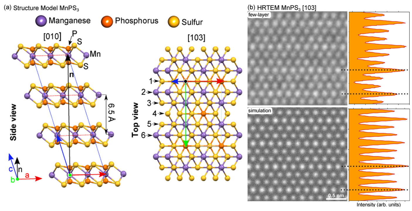
Crystal structure and thickness analysis
The researchers first checked what they were looking at: the orientation, thickness and quality of the transferred pristine flakes, which are known to oxidise easily[43]. Because MnPS3, FePS3 and NiPS3 share the same structure, the analysis of MnPS3 holds for all three. In the bulk, the layers are stacked with a lateral shift and follow monoclinic symmetry[45] (Fig. 1a). All HRTEM images show the flakes viewed perpendicular to the layers, along the [103] direction (Fig. 1b). The best match to the experimental image is a simulated crystal of four layers without stacking faults, and an independent TEM thickness measurement[46] gives about 3 nm. The team concluded that the pristine samples are few-layer systems of 3–6 layers with very good crystal quality and no stacking faults; the box below explains how the image reveals this.
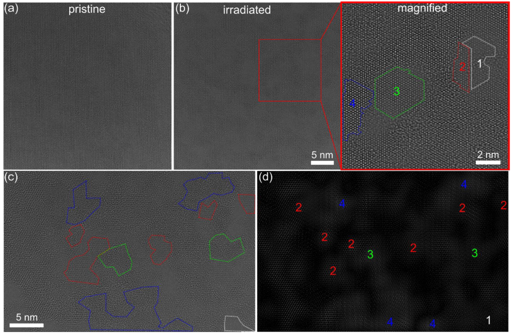
Interaction between electrons and sample
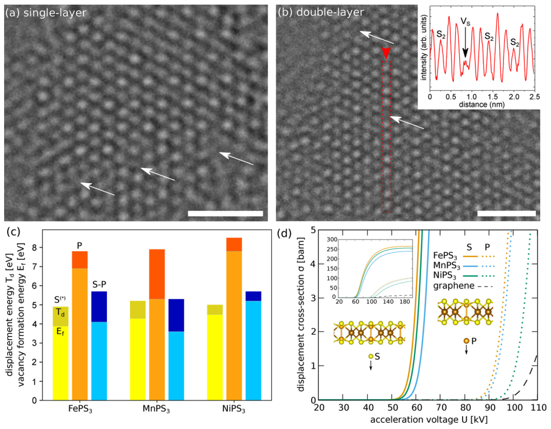
Under continuous irradiation the crystals give way layer by layer. Fig. 2 shows a four-layer NiPS3 region that thins step by step, leaving areas of three, two and one layer. Single defects appear in the layers along the way: the 80 kV HRTEM images of single- and double-layer NiPS3 in Fig. 3a and 3b show isolated vacancies, marked by white arrows. In the double layer, the contrast at one site disappears, as the line scan in the inset of Fig. 3b shows; the defect is a sulfur vacancy (VS) in an atomic column where the S atoms of the two layers sit on top of each other.
According to the experiments, sulfur or phosphorus vacancies form first and later grow into larger defects or even holes. To understand why, the team computed the displacement thresholds Td of S and P atoms in single-layer TMPTs with ab initio molecular dynamics (Fig. 3c), as well as the cross sections for knock-on damage (Fig. 3d). The threshold for sulfur turned out to be clearly lower than that for phosphorus, and much lower than for graphene, so elastic collisions at 50–300 kV should remove more S than P. Inelastic scattering, known to matter in 2D insulators and semiconductors[47]–[50], adds further damage channels; in single-layer MoS2 they create single S vacancies even at electron energies well below the knock-on threshold[47],[48],[51]. Since sulfur is also three times more abundant than phosphorus, the high-energy electrons (20–300 kV) should remove it easily, and strong structural changes are expected in few-layer systems as well. Imaging 2D materials entirely without beam–sample interaction may indeed be impossible[52]. The box below explains how the thresholds and cross sections were obtained.
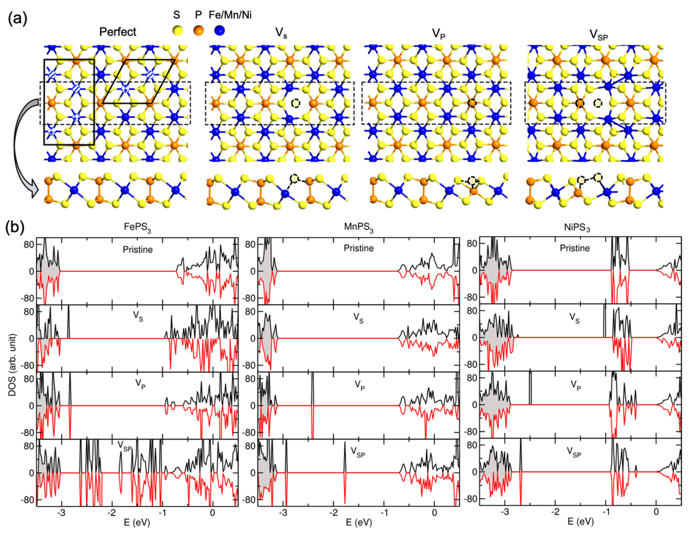
Defects also change what the material does electronically. Density functional theory (DFT) calculations showed that pristine TMPT single layers are semiconductors with band gaps of 2.0–2.3 eV, and that vacancies add new states in or near the gap (Fig. 4). Removing atoms is therefore a handle on the electronic properties, as the following box shows.
Electron beam excited chemical and structural changes analyzed with EELS and EDX
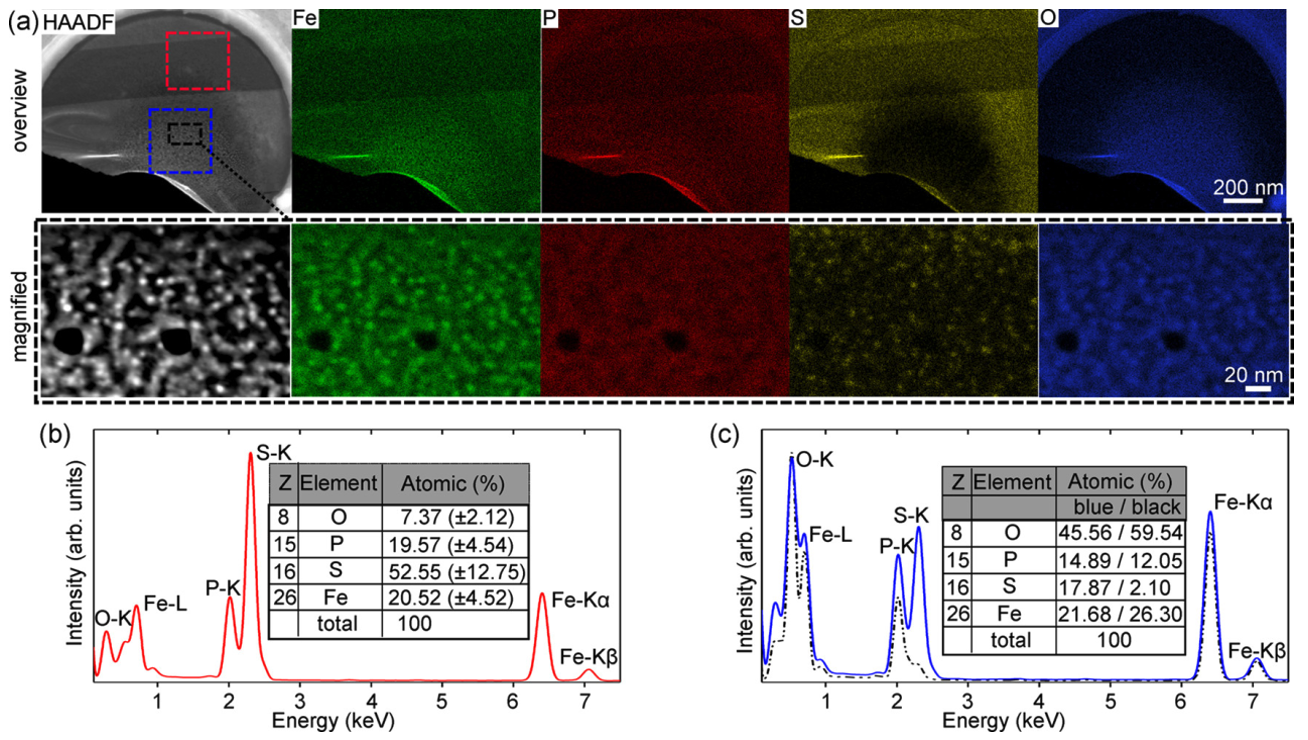
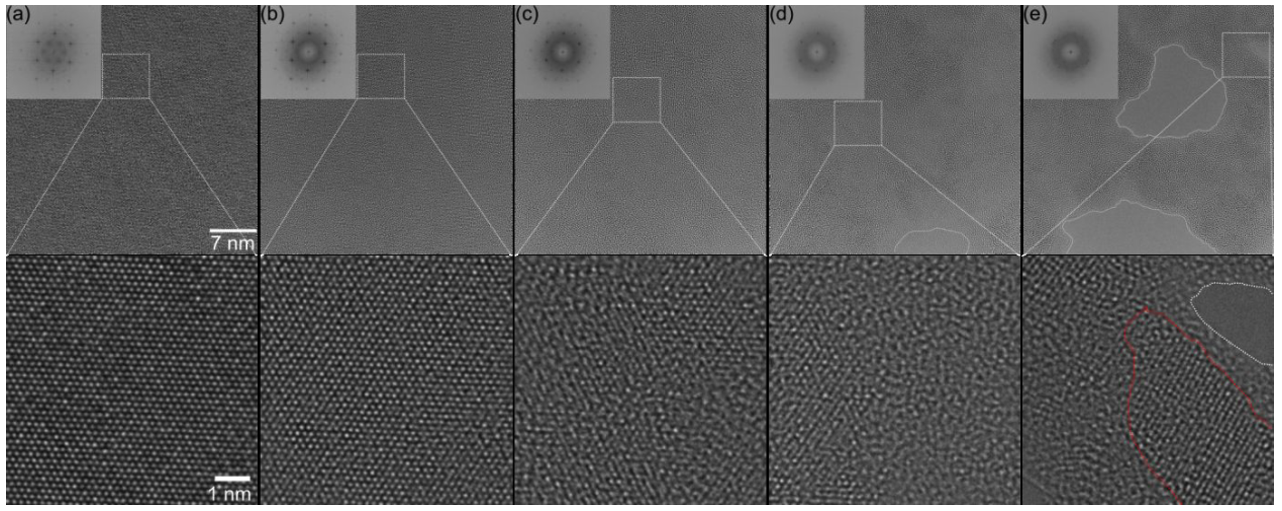
To follow the chemistry, the researchers looked in detail at FePS3; MnPS3 and NiPS3 behaved in the same way unless noted otherwise. Fig. 5 shows an 80 kV high-angle annular dark-field (HAADF) image of an irradiated and an unirradiated region with the elemental maps of Fe, P, S and O. The irradiated region becomes disordered and forms clusters, as the magnified area in Fig. 5a and the HRTEM series in Fig. 6 show: first single atoms go missing, then the atomic columns deform, the crystal dissolves, holes open and the remaining material gathers into clusters. Comparing the atomic fractions of both regions confirmed that mainly sulfur is removed, in line with the calculations (Fig. 5b,c).
To compare with these images, the team modelled phases of intermediate stoichiometry that could form as sulfur is lost, by spreading vacancies evenly through the pristine structure as under prolonged irradiation. At sulfur vacancy concentrations above 50 %, the optimised structures showed the same clustering of metal atoms as the experiment. Such non-stoichiometric phases can be stabilised in the metal-rich regime, as shown earlier for transition metal dichalcogenides[58]. With more sulfur vacancies, the number of mid-gap states grew, and their position depended on how the defects were distributed. Eventually the states are expected to fill the whole band gap, so the irradiated samples may show hopping-type conductivity.
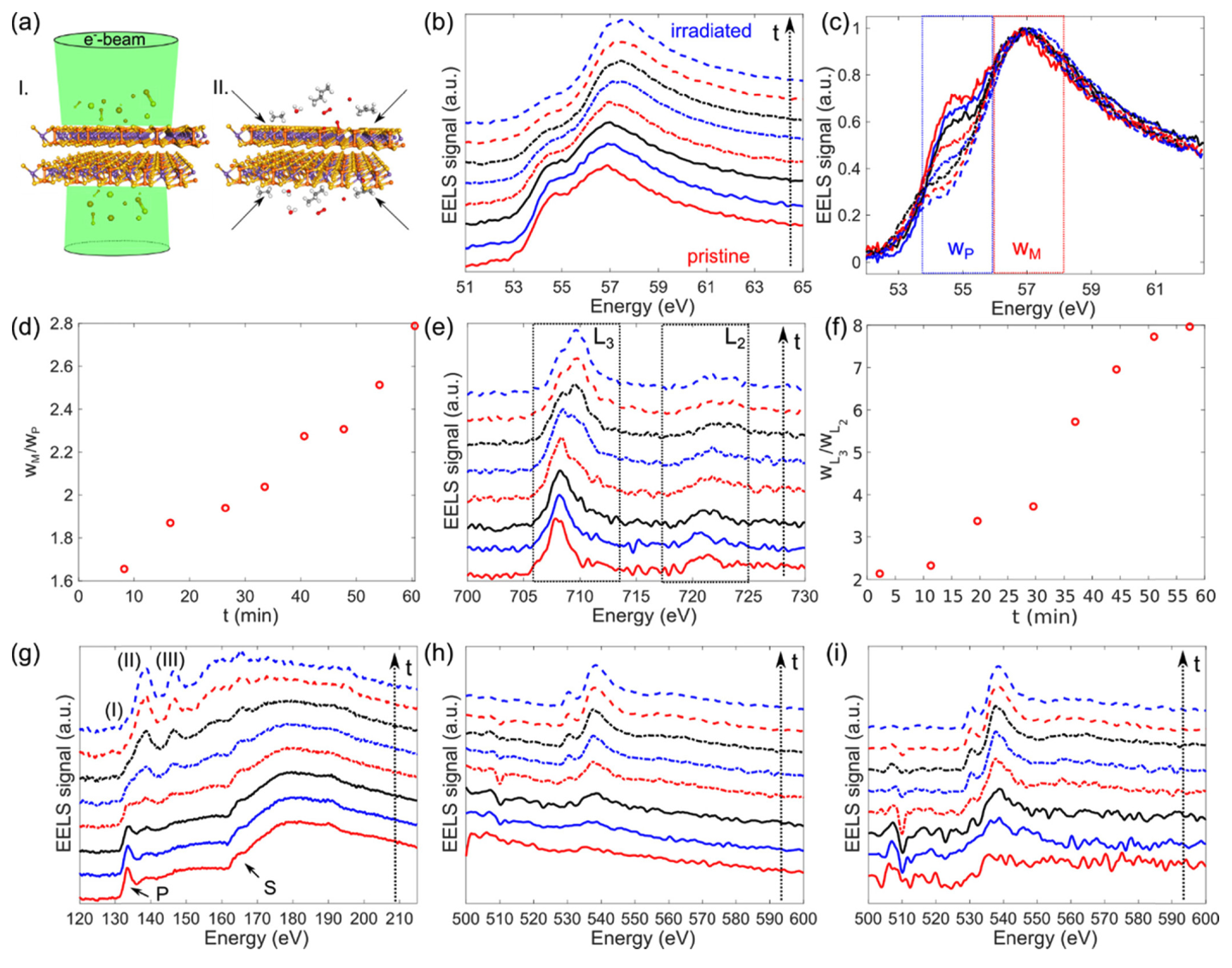
The conversion itself (Fig. 7a) was followed with the energy-loss near-edge structure (ELNES) of the core-loss edges, the fine structure that reveals bonding and oxidation states. The team recorded EELS spectra over 60 minutes at a constant, low dose rate of 15 × 103 e−/(s·nm2) and tracked how they evolved (Fig. 7). Both iron edges showed the same trend: the iron in pristine FePS3 is mainly divalent (Fe2+), as expected for this compound[59], and it gradually turned trivalent (Fe3+) under the beam. At the phosphorus edge, the signal of the P–S bond faded and two new peaks appeared, while the phosphorus contributions grew relative to sulfur, again showing that mostly sulfur leaves. The box below explains how the edges were read.
The oxygen came from two sources: residual contamination on the surface and the residual gas in the microscope column, which the condensed beam ionises; even the carbon mesh of the TEM grid carries an oxygen signal. The damaged material is all the more prone to oxidation and pulls the oxygen towards the illuminated area, which matches the high oxygen content that EDX found there (Fig. 5). The new peaks at 138.5 and 146.5 eV fit earlier reports of P–O bonds in oxidised phosphorus compounds[67], so the accumulated oxygen binds to the remaining phosphorus, and together with the Fe2+ → Fe3+ shift in EELS (Fig. 7) and the EDX maps (Fig. 5) the data show oxygen bound to iron as well. The exact local stoichiometry and structure of the oxidised material could not be identified. Irradiation at 30 and 60 kV gave similar results for MnPS3: again mainly sulfur and some phosphorus were removed, oxygen accumulated, and the residual P and Mn clustered together with O.
The study shows that ternary TMPTs have much lower knock-on thresholds than graphene and many binary transition metal dichalcogenides, that sulfur leaves first, and that the resulting vacancies add new states to the band gap and, depending on the sulfur content, magnetism from asymmetric spin polarisation. The experiments also illustrate, as the authors write, “the sensitivity of TMPTs to oxidation and the necessity to control the imaging conditions (i.e., dose rate as well as the irradiation time).” Controlled at the atomic scale in the Cc/Cs-corrected SALVE microscope at Ulm University, the electron beam thus becomes a tool: by setting how much sulfur remains, it opens a way to tailor the electronic and structural properties of freestanding few-layer TMPTs.
Resource:
Köster, J., Storm, A., Ghorbani-Asl, M., Kretschmer, S., Gorelik, T. E., Krasheninnikov, A. V., Kaiser, U. (2022).
Structural and Chemical Modifications of Few-Layer Transition Metal Phosphorous Trisulfides by Electron Irradiation.
J. Phys. Chem. C 126(36), 15446–15455.
https://doi.org/10.1021/acs.jpcc.2c03800
 Download this news article as PDF – for reading on paper, taking notes or filing.
-
Tang, K., Qi, W., Li, Y., Wang, T. (2018). Electronic Properties of van der Waals Heterostructure of Black Phosphorus and MoS2. J. Phys. Chem. C, 122, 7027–7032. https://doi.org/10.1021/acs.jpcc.8b01476
-
Chowdhury, T., Sadler, E. C., Kempa, T. J. (2020). Progress and Prospects in Transition-Metal Dichalcogenide Research Beyond 2D. Chem. Rev., 120, 12563–12591. https://doi.org/10.1021/acs.chemrev.0c00505
-
Zhao, B., Shen, D., Zhang, Z., Lu, P., Hossain, M., Li, J., et al. (2021). 2D Metallic Transition‐Metal Dichalcogenides: Structures, Synthesis, Properties, and Applications. Adv Funct Materials, 31, 2105132. https://doi.org/10.1002/adfm.202105132
-
Gong, C., Zhang, Y., Chen, W., Chu, J., Lei, T., Pu, J., et al. (2017). Electronic and Optoelectronic Applications Based on 2D Novel Anisotropic Transition Metal Dichalcogenides. Advanced Science, 4, 1700231. https://doi.org/10.1002/advs.201700231
-
Novoselov, K. S., Mishchenko, A., Carvalho, A., Castro Neto, A. H. (2016). 2D materials and van der Waals heterostructures. Science, 353, aac9439. https://doi.org/10.1126/science.aac9439
-
Zhang, S., Liu, J., Kirchner, M. M., Wang, H., Ren, Y., Lei, W. (2021). Two-dimensional heterostructures and their device applications: progress, challenges and opportunities—review. J. Phys. D: Appl. Phys., 54, 433001. https://doi.org/10.1088/1361-6463/ac16a4
-
Li, L., Shang, Y., Lv, S., Li, Y., Fang, Y., Li, H. (2021). Flexible and highly responsive photodetectors based on heterostructures of MoS2 and all-carbon transistors. Nanotechnology, 32, 315209. https://doi.org/10.1088/1361-6528/abf5ff
-
Wildes, A. R., Rule, K. C., Bewley, R. I., Enderle, M., Hicks, T. J. (2012). The magnon dynamics and spin exchange parameters of FePS3. J. Phys.: Condens. Matter, 24, 416004. https://doi.org/10.1088/0953-8984/24/41/416004
-
Liu, J., Li, X. B., Wang, D., Lau, W. M., Peng, P., Liu, L. M. (2014). Diverse and tunable electronic structures of single-layer metal phosphorus trichalcogenides for photocatalytic water splitting. The Journal of Chemical Physics, 140, 054707. https://doi.org/10.1063/1.4863695
-
Ismail, N., El-Meligi, A., Temerk, Y., Madian, M. (2010). Synthesis and characterization of layered FePS3 for hydrogen uptake. International Journal of Hydrogen Energy, 35, 7827–7834. https://doi.org/10.1016/j.ijhydene.2010.05.061
-
Du, K. z., Wang, X. z., Liu, Y., Hu, P., Utama, M. I. B., Gan, C. K., et al. (2016). Weak Van der Waals Stacking, Wide-Range Band Gap, and Raman Study on Ultrathin Layers of Metal Phosphorus Trichalcogenides. ACS Nano, 10, 1738–1743. https://doi.org/10.1021/acsnano.5b05927
-
Zhang, X., Zhao, X., Wu, D., Jing, Y., Zhou, Z. (2016). MnPSe3 Monolayer: A Promising 2D Visible‐Light Photohydrolytic Catalyst with High Carrier Mobility. Advanced Science, 3, 1600062. https://doi.org/10.1002/advs.201600062
-
Hashemi, A., Komsa, H. P., Puska, M., Krasheninnikov, A. V. (2017). Vibrational Properties of Metal Phosphorus Trichalcogenides from First-Principles Calculations. J. Phys. Chem. C, 121, 27207–27217. https://doi.org/10.1021/acs.jpcc.7b09634
-
Jenjeti, R. N., Kumar, R., Austeria, M. P., Sampath, S. (2018). Field Effect Transistor Based on Layered NiPS3. Sci Rep, 8, 8586. https://doi.org/10.1038/s41598-018-26522-1
-
Goossens, D. J. (2010). Dipolar anisotropy in quasi-2D honeycomb antiferromagnet MnPS3. Eur. Phys. J. B, 78, 305–309. https://doi.org/10.1140/epjb/e2010-10569-x
-
Mayorga-Martinez, C. C., Sofer, Z., Sedmidubský, D., Huber, Š., Eng, A. Y. S., Pumera, M. (2017). Layered Metal Thiophosphite Materials: Magnetic, Electrochemical, and Electronic Properties. ACS Appl. Mater. Interfaces, 9, 12563–12573. https://doi.org/10.1021/acsami.6b16553
-
Kim, T. Y., Park, C. H. (2021). Magnetic Anisotropy and Magnetic Ordering of Transition-Metal Phosphorus Trisulfides. Nano Lett., 21, 10114–10121. https://doi.org/10.1021/acs.nanolett.1c03992
-
Gibertini, M., Koperski, M., Morpurgo, A. F., Novoselov, K. S. (2019). Magnetic 2D materials and heterostructures. Nat. Nanotechnol., 14, 408–419. https://doi.org/10.1038/s41565-019-0438-6
-
Li, K., Chang, T., Xie, Q., Cheng, Y., Yang, H., Chen, J., et al. (2019). Tunable Magnetic Response in 2D Materials via Reversible Intercalation of Paramagnetic Ions. Adv Elect Materials, 5, 1900040. https://doi.org/10.1002/aelm.201900040
-
Clement, R. (1980). A novel route to intercalation into layered MnPS3. J. Chem. Soc., Chem. Commun., 647. https://doi.org/10.1039/c39800000647
-
Spodine, E., Valencia-Gálvez, P., Manzur, J., Paredes-García, V., Pizarro, N., Bernot, K., et al. (2012). Optical properties of composites formed by transition metal macrocyclic complexes intercalated in thiophosphate layered phases. Polyhedron, 44, 187–193. https://doi.org/10.1016/j.poly.2012.06.064
-
Spodine, E., Valencia-Gálvez, P., Fuentealba, P., Manzur, J., Ruiz, D., Venegas-Yazigi, D., et al. (2011). Magnetic behavior of MnPS3 phases intercalated by [Zn2L]2+ (LH2: macrocyclic ligand obtained by condensation of 2-hydroxy-5-methyl-1,3-benzenedicarbaldehyde and 1,2-diaminobenzene). Journal of Solid State Chemistry, 184, 1129–1134. https://doi.org/10.1016/j.jssc.2011.03.009
-
Jana, R., Chowdhury, C., Datta, A. (2020). Transition‐Metal Phosphorus Trisulfides and its Vacancy Defects: Emergence of a New Class of Anode Material for Li‐Ion Batteries. ChemSusChem, 13, 3855–3864. https://doi.org/10.1002/cssc.202001302
-
Wang, Y., Zhou, Z., Wen, T., Zhou, Y., Li, N., Han, F., et al. (2016). Pressure-Driven Cooperative Spin-Crossover, Large-Volume Collapse, and Semiconductor-to-Metal Transition in Manganese(II) Honeycomb Lattices. J. Am. Chem. Soc., 138, 15751–15757. https://doi.org/10.1021/jacs.6b10225
-
Yang, J., Zhou, Y., Guo, Q., Dedkov, Y., Voloshina, E. (2020). Electronic, magnetic and optical properties of MnPX3 (X = S, Se) monolayers with and without chalcogen defects: a first-principles study. RSC Adv., 10, 851–864. https://doi.org/10.1039/c9ra09030d
-
Murayama, C., Okabe, M., Urushihara, D., Asaka, T., Fukuda, K., Isobe, M., et al. (2016). Crystallographic features related to a van der Waals coupling in the layered chalcogenide FePS3. Journal of Applied Physics, 120, 142114. https://doi.org/10.1063/1.4961712
-
Wildes, A. R., Okamoto, S., Xiao, D. (2021). Search for nonreciprocal magnons in MnPS3. Phys. Rev. B, 103, 024424. https://doi.org/10.1103/physrevb.103.024424
-
Ju, H., Jeong, D. G., Choi, Y. G., Son, S., Jung, W. G., Jung, M. C., et al. (2020). Influence of stacking disorder on cross-plane thermal transport properties in TMPS3 (TM = Mn, Ni, Fe). Applied Physics Letters, 117, 063103. https://doi.org/10.1063/5.0013107
-
Zhao, X., Kotakoski, J., Meyer, J. C., Sutter, E., Sutter, P., Krasheninnikov, A. V., et al. (2017). Engineering and modifying two-dimensional materials by electron beams. MRS Bull., 42, 667–676. https://doi.org/10.1557/mrs.2017.184
-
Dash, A. K., Swaminathan, H., Berger, E., Mondal, M., Lehenkari, T., Prasad, P. R., et al. (2023). Evidence of defect formation in monolayer MoS2 at ultralow accelerating voltage electron irradiation. 2D Mater., 10, 035002. https://doi.org/10.1088/2053-1583/acc7b6
-
Björkman, T., Kurasch, S., Lehtinen, O., Kotakoski, J., Yazyev, O. V., Srivastava, A., et al. (2013). Defects in bilayer silica and graphene: common trends in diverse hexagonal two-dimensional systems. Sci Rep, 3, 3482. https://doi.org/10.1038/srep03482
-
Cretu, O., Komsa, H. P., Lehtinen, O., Algara-Siller, G., Kaiser, U., Suenaga, K., et al. (2014). Experimental Observation of Boron Nitride Chains. ACS Nano, 8, 11950–11957. https://doi.org/10.1021/nn5046147
-
Vasu, K. S., Prestat, E., Abraham, J., Dix, J., Kashtiban, R. J., Beheshtian, J., et al. (2016). Van der Waals pressure and its effect on trapped interlayer molecules. Nat Commun, 7, 12168. https://doi.org/10.1038/ncomms12168
-
Köster, J., Ghorbani-Asl, M., Komsa, H. P., Lehnert, T., Kretschmer, S., Krasheninnikov, A. V., et al. (2021). Defect Agglomeration and Electron-Beam-Induced Local-Phase Transformations in Single-Layer MoTe2. J. Phys. Chem. C, 125, 13601–13609. https://doi.org/10.1021/acs.jpcc.1c02202
-
Banhart, F., Kotakoski, J., Krasheninnikov, A. V. (2011). Structural Defects in Graphene. ACS Nano, 5, 26–41. https://doi.org/10.1021/nn102598m
-
Zhou, W., Zou, X., Najmaei, S., Liu, Z., Shi, Y., Kong, J., et al. (2013). Intrinsic Structural Defects in Monolayer Molybdenum Disulfide. Nano Lett., 13, 2615–2622. https://doi.org/10.1021/nl4007479
-
Susi, T., Kotakoski, J., Kepaptsoglou, D., Mangler, C., Lovejoy, T. C., Krivanek, O. L., et al. (2014). Silicon–Carbon Bond Inversions Driven by 60-keV Electrons in Graphene. Phys. Rev. Lett., 113, 115501. https://doi.org/10.1103/physrevlett.113.115501
-
Luo, C., Wang, C., Wu, X., Zhang, J., Chu, J. (2017). In Situ Transmission Electron Microscopy Characterization and Manipulation of Two‐Dimensional Layered Materials beyond Graphene. Small, 13, 1604259. https://doi.org/10.1002/smll.201604259
-
Lehnert, T., Ghorbani-Asl, M., Köster, J., Lee, Z., Krasheninnikov, A. V., Kaiser, U. (2019). Electron-Beam-Driven Structure Evolution of Single-Layer MoTe2 for Quantum Devices. ACS Appl. Nano Mater., 2, 3262–3270. https://doi.org/10.1021/acsanm.9b00616
-
Komsa, H. P., Kotakoski, J., Kurasch, S., Lehtinen, O., Kaiser, U., Krasheninnikov, A. V. (2012). Two-Dimensional Transition Metal Dichalcogenides under Electron Irradiation: Defect Production and Doping. Phys. Rev. Lett., 109, 035503. https://doi.org/10.1103/physrevlett.109.035503
-
Lehnert, T., Lehtinen, O., Algara–Siller, G., Kaiser, U. (2017). Electron radiation damage mechanisms in 2D MoSe2. Applied Physics Letters, 110, 033106. https://doi.org/10.1063/1.4973809
-
Zhang, J., Yu, Y., Wang, P., Luo, C., Wu, X., Sun, Z., et al. (2019). Characterization of atomic defects on the photoluminescence in two‐dimensional materials using transmission electron microscope. InfoMat, 1, 85–97. https://doi.org/10.1002/inf2.12002
-
Köster, J., Liang, B., Storm, A., Kaiser, U. (2021). Polymer-assisted TEM specimen preparation method for oxidation-sensitive 2D materials. Nanotechnology, 32, 075704. https://doi.org/10.1088/1361-6528/abc49e
-
Kretschmer, S., Lehnert, T., Kaiser, U., Krasheninnikov, A. V. (2020). Formation of Defects in Two-Dimensional MoS2 in the Transmission Electron Microscope at Electron Energies below the Knock-on Threshold: The Role of Electronic Excitations. Nano Lett., 20, 2865–2870. https://doi.org/10.1021/acs.nanolett.0c00670
-
Ouvrard, G., Brec, R., Rouxel, J. (1985). Structural determination of some MPS3 layered phases (M = Mn, Fe, Co, Ni and Cd). Materials Research Bulletin, 20, 1181–1189. https://doi.org/10.1016/0025-5408(85)90092-3
-
Malis, T., Cheng, S. C., Egerton, R. F. (1988). EELS log‐ratio technique for specimen‐thickness measurement in the TEM. J. Elec. Microsc. Tech., 8, 193–200. https://doi.org/10.1002/jemt.1060080206
-
de Graaf, S., Kooi, B. J. (2022). Radiation damage and defect dynamics in 2D WS2: a low-voltage scanning transmission electron microscopy study. 2D Mater., 9, 015009. https://doi.org/10.1088/2053-1583/ac3377
-
de Graaf, S., Ahmadi, M., Lazić, I., Bosch, E. G. T., Kooi, B. J. (2021). Imaging atomic motion of light elements in 2D materials with 30 kV electron microscopy. Nanoscale, 13, 20683–20691. https://doi.org/10.1039/d1nr06614e
-
Susi, T., Meyer, J. C., Kotakoski, J. (2019). Quantifying transmission electron microscopy irradiation effects using two-dimensional materials. Nat Rev Phys, 1, 397–405. https://doi.org/10.1038/s42254-019-0058-y
-
Egerton, R. (2021). Radiation Damage and Nanofabrication in TEM and STEM. Micros. Today, 29, 56–59. https://doi.org/10.1017/s1551929521000663
-
Chen, F. R., Van Dyck, D., Kisielowski, C., Hansen, L. P., Barton, B., Helveg, S. (2021). Probing atom dynamics of excited Co-Mo-S nanocrystals in 3D. Nat Commun, 12, 5007. https://doi.org/10.1038/s41467-021-24857-4
-
Kisielowski, C., Specht, P., Rozeveld, S. J., Kang, J., Fielitz, A. J., Barton, D., et al. (2021). Modulating Electron Beam–Sample Interactions in Imaging and Diffraction Modes by Dose Fractionation with Low Dose Rates. Microscopy and Microanalysis, 27, 1420–1430. https://doi.org/10.1017/S143192762101268X
-
Meyer, J. C., Eder, F., Kurasch, S., Skakalova, V., Kotakoski, J., Park, H. J., et al. (2012). Accurate Measurement of Electron Beam Induced Displacement Cross Sections for Single-Layer Graphene. Phys. Rev. Lett., 108, 196102. https://doi.org/10.1103/PhysRevLett.108.196102
-
McKinley, W. A., Feshbach, H. (1948). The Coulomb Scattering of Relativistic Electrons by Nuclei. Phys. Rev., 74, 1759–1763. https://doi.org/10.1103/physrev.74.1759
-
Mott, N. F. (1929). The scattering of fast electrons by atomic nuclei. Proceedings of the Royal Society of London. Series A, Containing Papers of a Mathematical and Physical Character, 124, 425–442. https://doi.org/10.1098/rspa.1929.0127
-
Susi, T., Hofer, C., Argentero, G., Leuthner, G. T., Pennycook, T. J., Mangler, C., et al. (2016). Isotope analysis in the transmission electron microscope. Nat Commun, 7, 13040. https://doi.org/10.1038/ncomms13040
-
Komsa, H. P., Krasheninnikov, A. V. (2012). Effects of confinement and environment on the electronic structure and exciton binding energy of MoS2 from first principles. Phys. Rev. B, 86, 241201. https://doi.org/10.1103/physrevb.86.241201
-
Joseph, T., Ghorbani-Asl, M., Kvashnin, A. G., Larionov, K. V., Popov, Z. I., Sorokin, P. B., et al. (2019). Nonstoichiometric Phases of Two-Dimensional Transition-Metal Dichalcogenides: From Chalcogen Vacancies to Pure Metal Membranes. J. Phys. Chem. Lett., 10, 6492–6498. https://doi.org/10.1021/acs.jpclett.9b02529
-
Brec, R. (1986). Review on structural and chemical properties of transition metal phosphorus trisulfides MPS3. In: Intercalation in Layered Materials, pp. 93–124. Springer, Boston, MA. https://doi.org/10.1007/978-1-4757-5556-5_4
-
van Aken, P. A., Styrsa, V. J., Liebscher, B., Woodland, A. B., Redhammer, G. J. (1999). Microanalysis of Fe3+/ΣFe in oxide and silicate minerals by investigation of electron energy-loss near-edge structures (ELNES) at the Fe M 2,3 edge. Physics and Chemistry of Minerals, 26, 584–590. https://doi.org/10.1007/s002690050222
-
Tan, H., Verbeeck, J., Abakumov, A., Van Tendeloo, G. (2012). Oxidation state and chemical shift investigation in transition metal oxides by EELS. Ultramicroscopy, 116, 24–33. https://doi.org/10.1016/j.ultramic.2012.03.002
-
van Aken, P. A., Liebscher, B., Styrsa, V. J. (1998). Quantitative determination of iron oxidation states in minerals using Fe L2,3-edge electron energy-loss near-edge structure spectroscopy. Physics and Chemistry of Minerals, 25, 323–327. https://doi.org/10.1007/s002690050122
-
van Aken, P. A., Liebscher, B. (2002). Quantification of ferrous/ferric ratios in minerals: new evaluation schemes of Fe L2,3 electron energy-loss near-edge spectra. Physics and Chemistry of Minerals, 29, 188–200. https://doi.org/10.1007/s00269-001-0222-6
-
Garvie, L., Craven, A. (1994). High-resolution parallel electron energy-loss spectroscopy of Mn L2,3-edges in inorganic manganese compounds. Phys Chem Minerals, 21. https://doi.org/10.1007/bf00202132
-
Schmid, H., Mader, W. (2006). Oxidation states of Mn and Fe in various compound oxide systems. Micron, 37, 426–432. https://doi.org/10.1016/j.micron.2005.12.004
-
Lau, W. M., Jin, S., Wu, X. W., Ingrey, S. (1990). In situ x-ray photoelectron spectroscopic study of remote plasma enhanced chemical vapor deposition of silicon nitride on sulfide passivated InP. Journal of Vacuum Science & Technology B: Microelectronics Processing and Phenomena, 8, 848–855. https://doi.org/10.1116/1.584977
-
Kruse, J., Leinweber, P., Eckhardt, K. U., Godlinski, F., Hu, Y., Zuin, L. (2009). Phosphorus L2,3-edge XANES: overview of reference compounds. J Synchrotron Rad, 16, 247–259. https://doi.org/10.1107/s0909049509000211