
Bottom-Up Nanocrystalline Graphene

January 2, 2026 – Researchers from Leiden University, Ulm University, TU Dresden, TU Darmstadt, the University of Groningen and Xi'an Jiaotong University have developed a bottom-up synthesis method for centimeter-sized nanocrystalline graphene monolayers by pyrolyzing a Langmuir monolayer of a polyaromatic hydrocarbon at the water-air interface. The resulting material is just 0.36 nm thick, comparable to single-layer graphene, and offers a modular strategy for designing nanocrystalline 2D films with potential applications in nanoelectronics and as free-standing membranes.
A single layer of carbon atoms is usually grown from simple gases, so its structure is set by the furnace rather than by chemistry. Carbon materials find use in a wide range of applications, including adsorption and membrane separation of gases and ions,[1] energy storage devices,[2] and chemical sensors,[3] and are usually prepared by pyrolysis of organic precursors. The engineering of bulk carbon materials is achieved through modulation of precursors' structure and stacking mode,[1] alongside optimization of pyrolysis conditions.[4] For 2D carbon materials such as graphene, amorphous carbon monolayer, and nanocrystalline graphene, however, the resulting film morphology is regulated mainly by pyrolysis conditions, for instance temperature,[5] pressure,[6] and flow rates.[7] Although many carbon precursors, such as methane, ethanol, and benzene, have been used for 2D carbon growth, tuning the resulting films through the molecular structure of the precursor has remained challenging: these processes use simple, volatile molecules, and the amount of carbon on the substrate cannot be controlled by their chemical structure. Recent theoretical and experimental studies show that when the grain size is reduced to a few nanometers, nanocrystalline graphene or amorphous carbon monolayers with many grain boundaries exhibit distinct electronic properties,[8],[9] making them interesting for fundamental research and technical applications. For instance, nanocrystalline graphene–MoS2 van der Waals (vdW) heterostructures show current rectification.
Nanocrystalline graphene monolayers with a controlled internal morphology would benefit from a modular, bottom-up approach. During the CVD growth of nanocrystalline graphene, the high concentration of active carbon species provides a high nucleation density and therefore the growth of multilayers, with an overall film thickness of more than a few nanometers.[10] Well-defined nanocrystalline graphene has been obtained by quenching a hot Pt foil in ethanol or by laser-assisted CVD growth on Cu,[5],[9] and self-assembled monolayers of aromatic thiols have proven very efficient for amorphous carbon films.[8],[11],[12] Recently, the team synthesized a molecularly thin amorphous carbon monolayer (2 nm thick) by pyrolyzing a Langmuir monolayer of the amphiphilic polyaromatic hydrocarbon (PAH) hexa(2,2'-dipyridylamino)hexabenzocoronene (HPAHBC).[13],[14] This non-volatile, highly thermally stable PAH monolayer served as the carbon source. Its molecules, however, stand edge-on on the water and later on the substrate, held by π-π stacking and by hydrogen bonds between water and their pyridine groups.
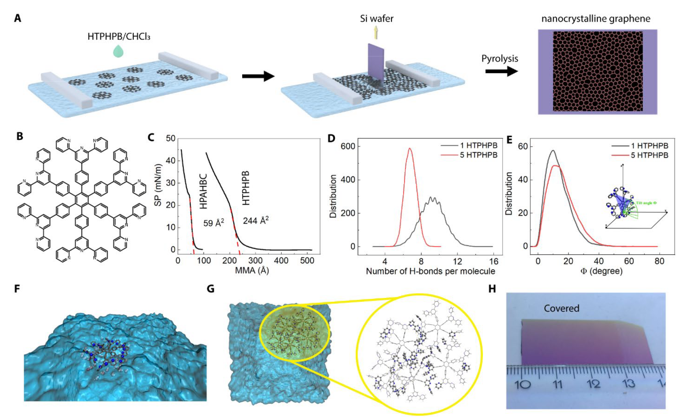
The new route lies these molecules flat. The team prepared a centimeter-sized nanocrystalline graphene monolayer by pyrolyzing, under an inert atmosphere, a Langmuir monolayer of hexa(terpyridine)hexaphenylbenzene (HTPHPB), a PAH with a less conjugated core (Fig. 1A-B). The mean molecular area obtained from the compression isotherm, about 244 Å2, is close to the size of HTPHPB calculated from its single crystal structure, indicating that the monomers adopted a face-on configuration on the water surface (Fig. 1C). The preparation is summarized in the box below.
Simulations explained why the molecules lie flat. Molecular dynamics (MD) showed that hydrogen bonds between water and the pyridine groups dominate the arrangement at the interface: a single HTPHPB molecule forms on average 9 hydrogen bonds and lies nearly flat, tilted by only ~13° (Fig. 1D-F). This contrasts with the earlier HPAHBC,[13] where π-π stacking between the large coronene cores competed with the hydrogen bonds. The details are in the box below.
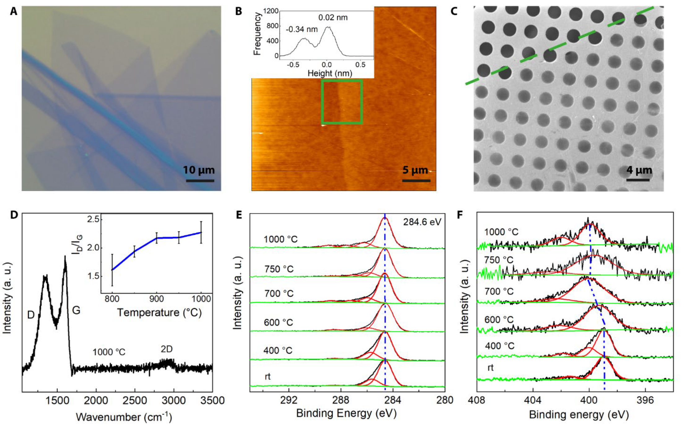
After annealing on the Si wafer, the nanocrystalline graphene monolayer gives a similar optical contrast as monolayer graphene (Fig. 1H, Fig. 2A). It measures 0.36 nm in thickness with an average roughness (Ra) of 0.07 nm (Fig. 2B), the same thickness as single-layer graphene and thinner than an amorphous carbon monolayer,[5] which shows its atomically thin nature. Transferred onto a Quantifoil grid, the monolayer is mechanically strong enough to be free-standing over openings of at least 2 μm (Fig. 2C).
The annealing temperature must be high enough to rearrange the carbon atoms. Raman spectroscopy showed that the conjugated structure first emerges at about 700 °C, and the weak 2D peak revealed a lack of long-range order even up to 1000 °C (Fig. 2D); the D/G intensity ratio indicates an average defect distance of around 1.5 nm. X-ray photoelectron spectroscopy (XPS) confirmed the transition. The box below gives the spectra in detail.

Spectroscopy averages over large areas, so the local structure of the annealed monolayers remained elusive. The team therefore imaged the atoms with aberration-corrected high-resolution transmission electron microscopy (AC-HRTEM). Selected-area electron diffraction shows two diffuse rings at 4.7 nm−1 and 8.1 nm−1, coinciding with graphitic carbon; their diffuse nature confirms the lack of long-range order seen by Raman spectroscopy. Fig. 3A presents a typical AC-HRTEM image of the monolayer annealed at 1000 °C, compared with CVD graphene (Fig. 3F). Thanks to the correction of chromatic and spherical aberrations, the instrumental resolution reaches 80 pm at 80 kV, so every carbon atom is resolved unambiguously.
Because the atoms are disordered, quantitative structural analysis of bond lengths, bond angles and the frequency of polygons is not a trivial task. The researchers therefore used a neural network based on the U-net architecture that determines the atomic positions in AC-HRTEM images automatically.[22] From the position of every single atom, the distributions of bond length and angle and the polygon percentages follow statistically; Fig. 3B shows the resulting polygon map. Segmentation in the network excludes non-monolayer regions caused by surface contamination and local thickness variation.
Evaluating 34 AC-HRTEM images with a 29 nm × 29 nm field of view, the researchers found that the bond length and angle distributions of nanocrystalline graphene (Figs. 3C-3D) are substantially broader than those of CVD graphene (Figs. 3G-3I). The full width at half maximum (FWHM) of the bond angle distribution increased from 16.3° (CVD graphene) to 24.0°, and that of the bond length distribution from 0.27 Å to 0.39 Å, while the peaks remain centered at 120° and 1.4 Å, the signature of sp2 carbon with short-range order. The polygon statistics (Fig. 3E) show a substantial increase in pentagons at the cost of hexagons compared with CVD graphene (Fig. 3J), whereas heptagons increased only slightly.
With higher annealing temperature, a larger fraction of monolayer (sp2) regions was observed, and the grain size measures around 2 nm, similar to in situ annealing of nanocrystalline graphene in the TEM. Although annealing above 700 °C already fully decomposes the pyridine motifs and triggers atomic rearrangement, the remaining carbon atoms first adopt a highly disordered configuration and serve as an ultrathin carbon reservoir. Further heating drives them into an energetically favorable crystalline state, forming the nanocrystalline graphene monolayer.
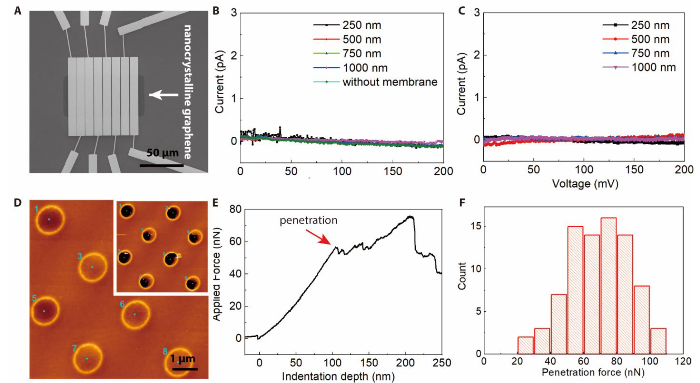
Because the monolayer grows directly on an insulating Si wafer, its resistance can be measured without transfer (Fig. 4A). Unlike graphene, with its high electron mobility and low resistance, the monolayers prepared at 750 °C and 1000 °C are insulators (Figs. 4B-4C): the current at 200 mV is below 1 pA and noisy, and the resistance exceeds 10 TΩ sq−1, the highest value reported so far among 2D carbon membranes.[5],[9] Compared with monolayer amorphous carbon films and nanocrystalline graphene reported in the literature,[5],[23] this is likely due to the inert Si wafer substrate, on which a high density of defects cannot be repaired during high-temperature growth. AFM nanoindentation over 1.2 μm holes confirmed the good mechanical properties of the free-standing film (Figs. 4D-4F).
Under a focused blue laser, the film prepared at 750 °C was etched away within about 6 s, whereas pristine graphene showed no change even after 10 min; the film prepared at 1000 °C was slightly more stable. The etching results from thermal oxidation and sublimation.[24] The difference to pristine graphene can be attributed to the abundance of grain boundaries and the small grain size, which largely decrease the thermal conductivity.[25] This low stability allows the film to be patterned directly on the wafer by laser scanning.
The study shows that the thickness of a 2D carbon film can be set by the design of its molecular precursor: HTPHPB, with its less conjugated core, lies flat on water and turns into carbon only one atom thick. The authors conclude that the film's "atomic thin nature" makes it "potentially useful as a free-standing membrane and in nanoelectronics", and its sensitivity to laser light may be useful for lithography. Since the film grows directly on a Si/SiO2 wafer, no transfer step is needed before device integration. The atom-by-atom view of its grains came from aberration-corrected HRTEM with the SALVE instrument at Ulm University.
Resource:
Liu, X., Calvani, D., Leist, C., Makurat, M., Melcrová, A., He, M., Scholma, D., Sevink, G. J. A., Buda, F., Hermans, Y., Hofmann, J. P., Qi, H., Feng, X., Roos, W. H., Kaiser, U., Schneider, G. F. (2026).
Monolayer nanocrystalline graphene synthesized from pyrolyzing a Langmuir monolayer of a polyaromatic hydrocarbon.
Sci. Adv. 12(1), eadv1856.
https://doi.org/10.1126/sciadv.adv1856
 Download this news article as PDF – for reading on paper, taking notes or filing.
-
Zhou, S. et al. (2024). Adsorption mechanism of CO2/CH4 in kaolinite clay: insight from molecular simulation. Energy Fuels, 33, 6542-6551. https://doi.org/10.1021/acs.energyfuels.9b00539
-
Liu, R. et al. (2015). A bottom-up synthesis of nitrogen-doped porous carbon for supercapacitors. Carbon, 81, 620-628. https://doi.org/10.1016/j.carbon.2014.10.001
-
Wang, X. et al. (2018). A novel humidity sensor based on honeycomb-like porous carbon derived from bio-waste. Sens. Actuators B Chem., 260, 1098-1105. https://doi.org/10.1016/j.snb.2018.01.114
-
Wang, Q., Yan, J., Wang, Y., Wei, T., Zhang, M., Jing, X. & Fan, Z. (2014). Three-dimensional flower-like and hierarchical porous carbon materials as high-rate performance electrodes for supercapacitors. Carbon, 67, 119-127. https://doi.org/10.1016/j.carbon.2013.09.070
-
Toh, C. T. et al. (2020). Synthesis and properties of free-standing monolayer amorphous carbon. Nature, 577, 199-203. https://doi.org/10.1038/s41586-019-1871-2
-
Dong, J. et al. (2023). Ultrathin nanocrystalline/amorphous carbon films with tailored sp3/sp2 bonding grown by physical vapor deposition. Carbon, 213, 118292. https://doi.org/10.1016/j.carbon.2023.118292
-
Zhou, Y., Loh, K. P. & Lin, J. (2018). Synthesis of graphene from acetylene via chemical vapor deposition: Growth mechanism and effects of hydrogen and carrier gas. Carbon, 126, 165-175. https://doi.org/10.1016/j.carbon.2017.10.022
-
Turchanin, A. & Golzhauser, A. (2012). Carbon nanomembranes from self-assembled monolayers: functional surfaces without bulk. Prog. Surf. Sci., 87, 108-162. https://doi.org/10.1016/j.progsurf.2012.05.001
-
Hong, J.-Y. et al. (2021). Monolayer nanocrystalline graphene from a liquid precursor. Nanoscale, 13, 12677-12687. https://doi.org/10.1039/D1NR02689J
-
Lee, J.-H. et al. (2014). Wafer-scale growth of single-crystal monolayer graphene on reusable hydrogen-terminated germanium. Science, 344, 286-289. https://doi.org/10.1126/science.1252268
-
Nottbohm, C. T. et al. (2011). Novel carbon nanosheets as support for ultrahigh-resolution structural analysis of nanoparticles. Ultramicroscopy, 111, 417-422. https://doi.org/10.1016/j.ultramic.2010.12.010
-
He, M., Guo, X. & Qi, H. (2023). Shaping 2D materials by radiation. Nat. Rev. Phys., 5, 662-681. https://doi.org/10.1038/s42254-023-00649-x
-
Liu, X. et al. (2022). Pyrolysis of a Langmuir monolayer to molecularly thin amorphous carbon. Nanoscale, 14, 13070-13079. https://doi.org/10.1039/D2NR03206H
-
Liu, X. et al. (2023). In situ visualization of pore evolution in monolayer amorphous carbon membranes. 2D Mater., 10, 011001. https://doi.org/10.1088/2053-1583/aca666
-
Gu, Y. et al. (2016). Flexible electronic eardrum. Nano Res., 10, 2683-2691. https://doi.org/10.1007/s12274-017-1470-1
-
Schlütter, F. et al. (2014). π-Conjugated heterotriangulene macrocycles by solution and surface-supported synthesis toward honeycomb networks. J. Am. Chem. Soc., 136, 8946-8953. https://doi.org/10.1021/ja502910y
-
Tsuzuki, S., Honda, K., Uchimaru, T. & Mikami, M. (2005). Ab initio calculations of structures and interaction energies of toluene dimers including CCSD(T) level electron correlation correction. J. Chem. Phys., 122, 144323. https://doi.org/10.1063/1.1876092
-
Malaspina, T., Coutinho, K. & Canuto, S. (2002). Ab initio calculation of hydrogen bonds in liquids: A sequential Monte Carlo quantum mechanics study of pyridine in water. J. Chem. Phys., 117, 1692-1699. https://doi.org/10.1063/1.1485963
-
Ma, Z. et al. (2015). Sulfur-doped graphene derived from cycled lithium–sulfur batteries as a metal-free electrocatalyst for the oxygen reduction reaction. Angew. Chem. Int. Ed., 54, 1888-1892. https://doi.org/10.1002/anie.201410258
-
Lucchese, M. M. et al. (2010). Quantifying ion-induced defects and Raman relaxation length in graphene. Carbon, 48, 1592-1597. https://doi.org/10.1016/j.carbon.2009.12.057
-
Araujo, P. T., Terrones, M. & Dresselhaus, M. S. (2012). Defects and impurities in graphene-like materials. Mater. Today, 15, 98-109. https://doi.org/10.1016/S1369-7021(12)70045-7
-
Leist, C., He, M., Liu, X., Kaiser, U. & Qi, H. (2022). Deep-learning pipeline for statistical quantification of amorphous two-dimensional materials. ACS Nano, 16, 20488-20496. https://doi.org/10.1021/acsnano.2c06807
-
Tian, H. et al. (2023). Disorder-tuned conductivity in amorphous monolayer carbon. Nature, 615, 56-61. https://doi.org/10.1038/s41586-022-05617-w
-
Lin, L. et al. (2018). Optothermoplasmonic nanolithography for on-demand patterning of 2D materials. Adv. Funct. Mater., 28, 1803990. https://doi.org/10.1002/adfm.201803990
-
Liu, H. K., Lin, Y. & Luo, S. N. (2014). Grain boundary energy and grain size dependences of thermal conductivity of polycrystalline graphene. J. Phys. Chem. C, 118, 24797-24802. https://doi.org/10.1021/jp508035b