Third SALVE symposium 2017 held at the University of Ulm

Figure 1: Symposium announcement
December 12-14, 2017 - The SALVE (Sub-Ångstrom Low Voltage Electron microscopy) Symposium 2017, organized by Ute Kaiser, was held from 12th to 14th of December just after the festive inauguration ceremony of the SALVE instrument in its new purpose-designed building on the 11th of December, 2017 (see the Newsarticle). The symposium brought together distinguished scientists from 17 countries (Fig. 2). After the opening of the symposium, Harald Rose showed in detail the development of aberration correction from its start with Otto Scherzer, his doctor father, until the SALVE Cc/Cs aberration corrector. At the end of the symposium, Ute Kaiser reviewed the transformations in the field of aberration-corrected low-voltage TEM and STEM in general and demonstrated, which questions can be addressed in this new, fast developing field. In the talks of the SALVE Team members, a particular focus was given to the outline and purpose of the new SALVE instrument and what it can contribute to the scientific community also in comparison to the other instruments.
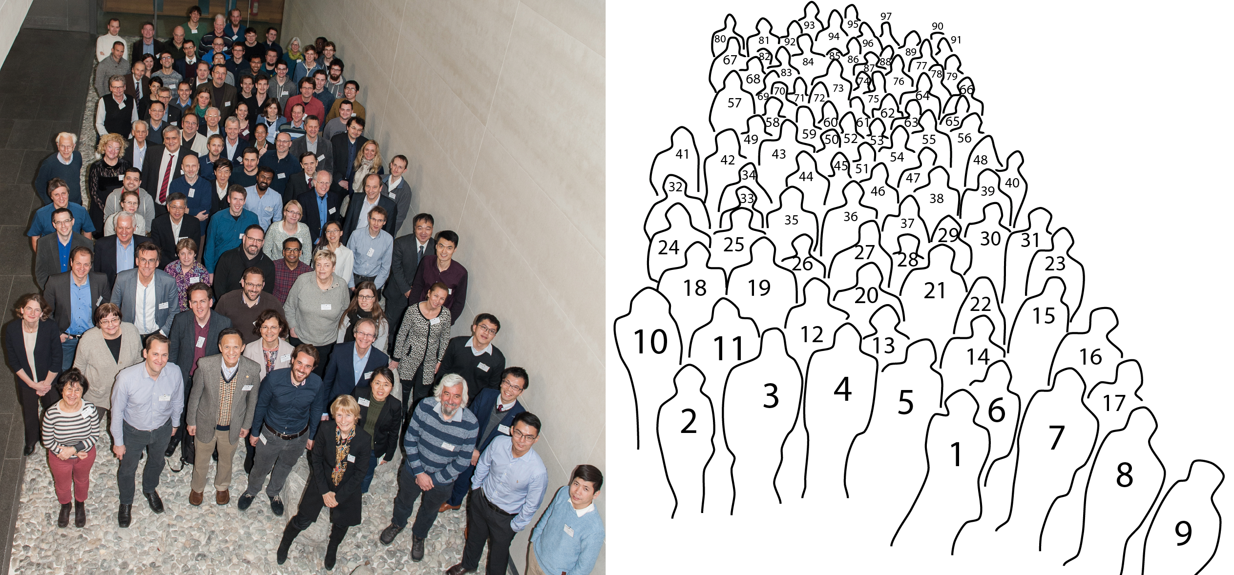
Figure 2: Group photo of the Third International SALVE Symposium 2017 with participants from 17 countries (to see the name of all participants click on the image).
The meeting consisted of 4 sessions: "Advanced Instrumentation", "Low-Dimensional Materials: Preparation, Characterization, Theory", and "Bridging Biological and Materials Science", and "Advanced techniques". This included topics as the manufacturing of low-dimensional materials, the assessment of their properties by theoretical calculations and the various TEM techniques (S)TEM imaging, in-situ TEM, electron holography, cryo-TEM and spectroscopy. Moreover, challenges and prospects of low-voltage imaging of biologically relevant objects were addressed.
The meeting finished with a round table discussion where the participants lively discussed the outcome of the symposium and the most important steps for the further advancement of low-voltage electron microscopy.
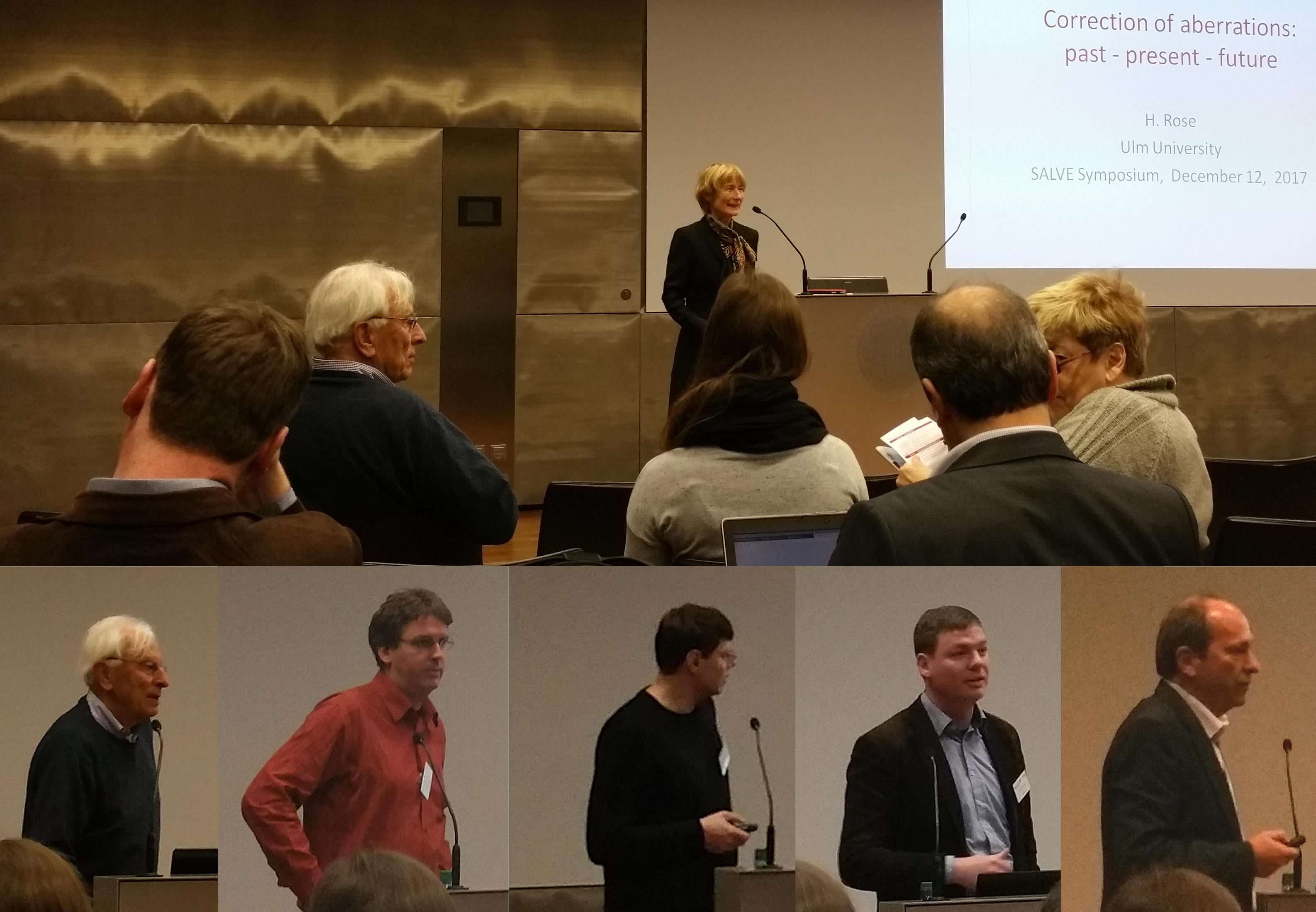
Figure 3: Session instrumentation I.
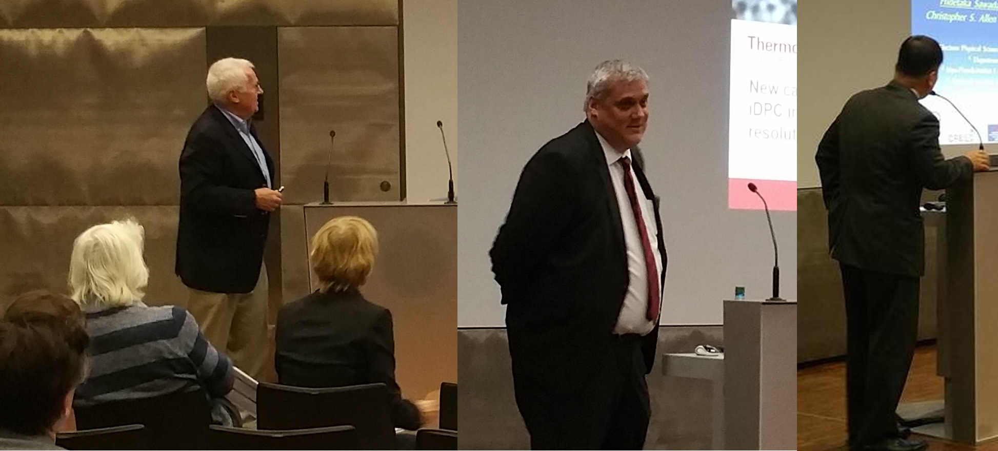
Figure 4: Session instrumentation II.
Sessions 1 “Advanced Instrumentation (I-II)” chaired by Ute Kaiser (Ulm University) and Max Haider (CEOS GmbH)
LV-AC-TEM is necessarily based on a change in instrumentation from medium voltage AC-TEM: reduction of the accelerating voltage. It is one of the most important measures to reduce radiation damage in TEM and requires either Cs-correction and dedicated monochromatization or Cc/Cs-correction. The results achieved so far since the beginning of the SALVE project and in the parallel low-voltage research projects in the last year and the future plans were discussed.
Prof. Harald Rose (Ulm University) presented status and future challenges of aberration-corrected electron microscopy. He showed what knowledge had to be produced from the very beginning of aberration correction up to the SALVE project. Dr. Heiko Müller (CEOS GmbH, Germany) presented the benchmarks of the Cc/Cs-corrected SALVE III microscope and revisited the different resolution-limiting factors at low accelerating voltages. With this instrument e.g. at 40 kV an information limit of 90 pm was demonstrated, which is only about fifteen times the electron wavelength and corresponds to an effective optical aperture of 67 mrad. Dr. Müller demonstrated further that due to the chromatic correction, defocus varies slowly with respect to the energy dispersion, which allows EFTEM imaging by using a large energy window without obvious loss of resolution. The development of in-column or post-column imaging energy filters in the future would be very compatible with this new technique of LV-AC-TEM down to 20 kV.
In the following talk, Dr. Johannes Biskupek (Uni Ulm, Germany) presented The EFTEM experiments supporting the conclusion of the previous talk, where a 10 eV window is applied for core-loss imaging of graphene, and the inelastic signal could be captured at the K-edge for the first time. Dr. Felix Börrnert (Uni Ulm, Germany) discussed the combined effect of lowering the electron energy and using the new chromatic aberration correction technology on the different information dampening envelope functions as well as on the coherent phase contrast transfer. These effects were discussed on the example of atomically resolved graphene images at acceleration voltages of 20 and 80 kV.
The results with Cc/Cs-correction in the EFTEM imaging at 80 kV have been compared by Prof. Joachim Mayer (Forschungszentrum Juelich, Germany and RWTH Aachen, Germany) with the Cc/Cs-corrected PICO microscope on the example of the silicon energy loss L2,3 edge, where a resolution of 135 pm has been achieved.
The companies Gatan, JEOL, Nion, and ThermoFisher Scientific (formerly FEI) presented their latest developments related to low-voltage TEM/STEM imaging. As an alternative to Cc-correction, monochromatization has demonstrated experimental success for STEM; Dr. Hidetaka Sawada (JEOL, Japan) reported on the Triple-C microscope operated at 15 kV and 60 kV. The point resolution reaches 120 pm at 15 kV with an energy width of 0.05 eV and 107 pm at 60 kV with an energy width of 0.2 eV. By monochromatization to 100 meV Prof. Ondrej Krivanek (Nion, USA) reported a point resolution of 107 pm at 30 kV. He pointed out that such a small energy window improves the information limit on the one hand, and indicates high input of electron dose for a sufficient signal-to-noise ratio on the other hand. The new capabilities of the Themis platform, which is the basis of the SALVE microscope, have been presented by Dr. Bert Freitag (Thermo-Fisher Scientific, USA/Netherlands) and recent progress in EELS detectors.
Axel Lubk (IFW Dresden, Germany) presented the latest instrumentation developments carried out at IfW Dresden where electron holography and tomography have been combined. By using their new reconstruction methods, technological limitations lying in the spatial resolution and the alignment of tilt series have been overcome, also thanks to a new specimen holder.
Figure 5: Session Materials 1.
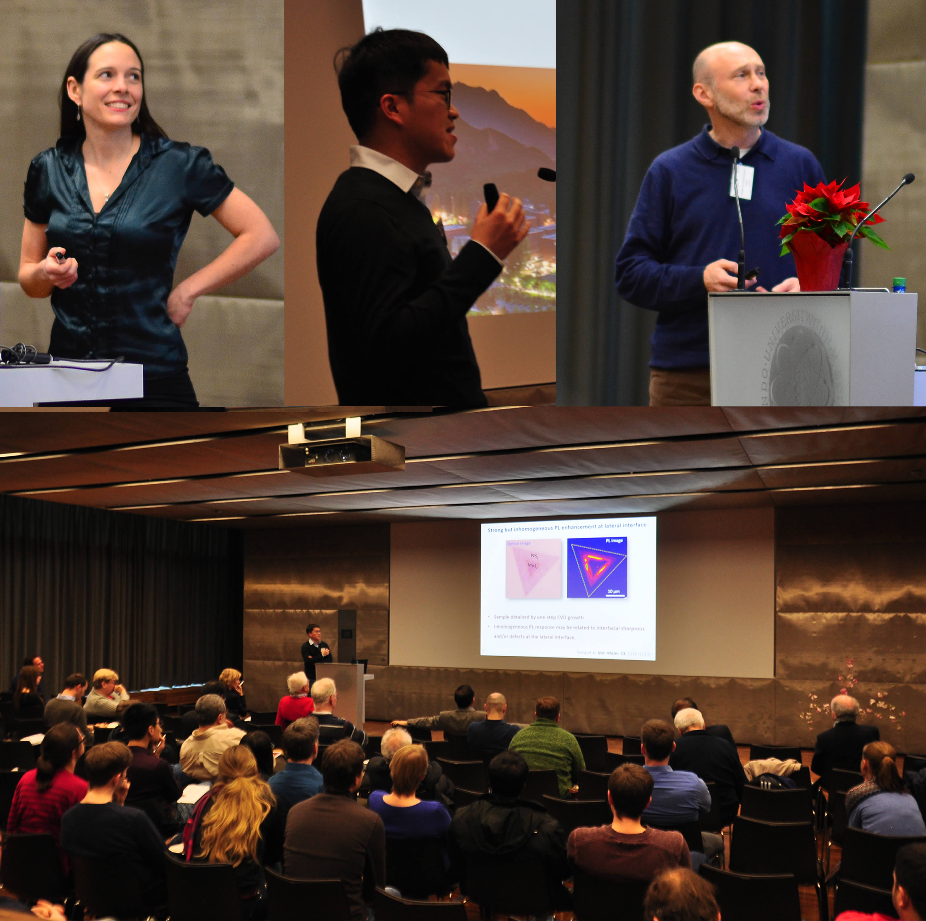
Figure 6: Session Materials 3.
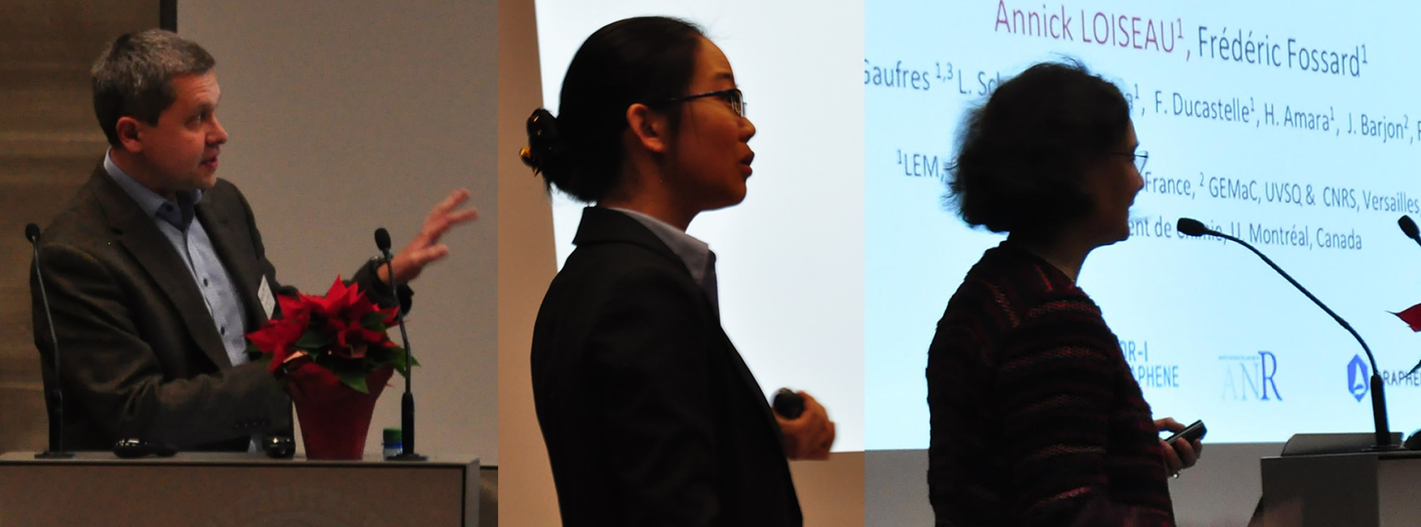
Figure 7: Session Materials 4.
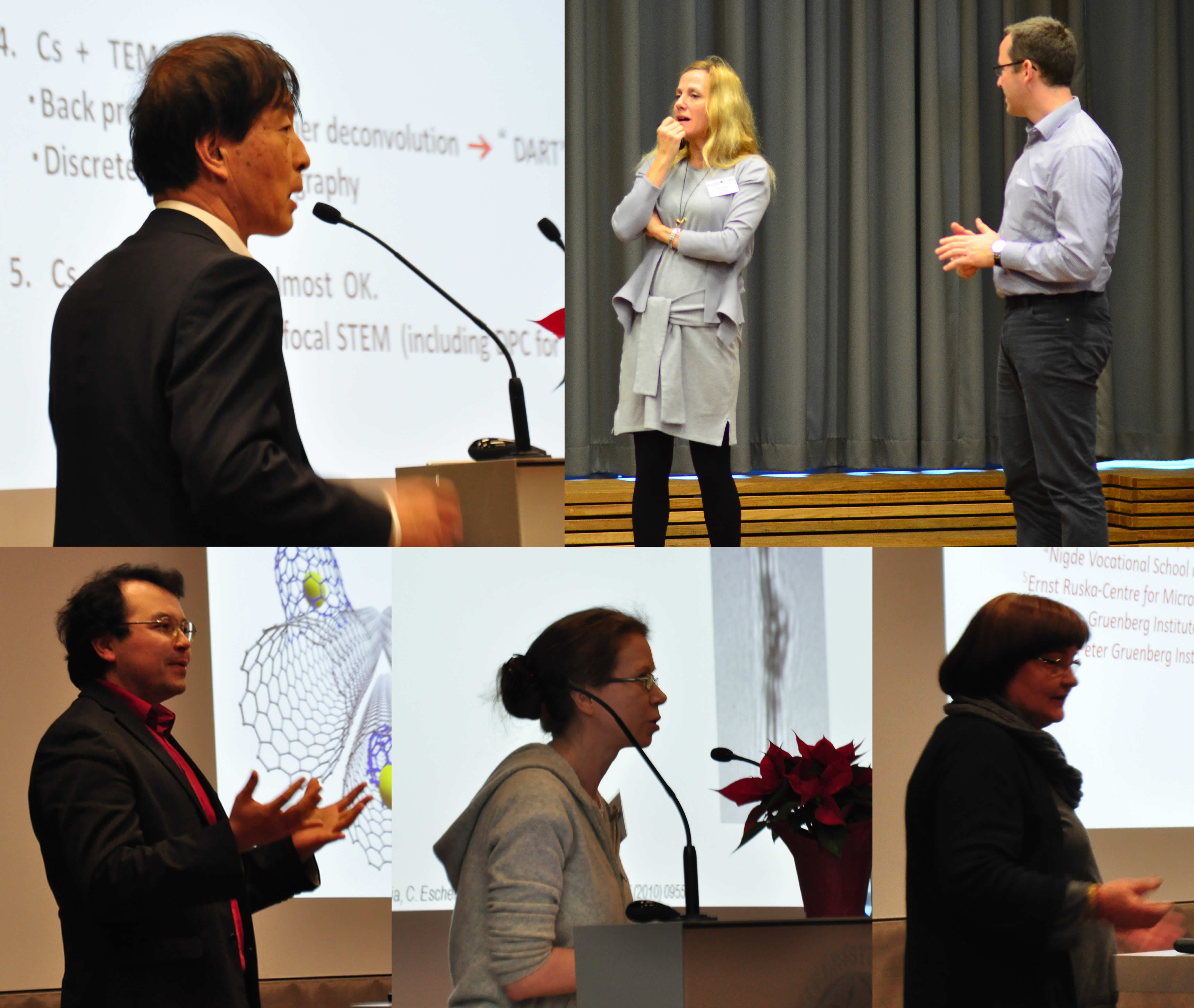
Figure 8: Session Materials 5.
Sessions 2 “Low-Dimensional Materials: Preparation, Characterization, Theory (I-V)” chairs: Eva Olsen (Chalmers University), Nobuo Tanaka (Nagoya University, Japan), Jannik Meyer (University Vienna, Austria), Frances Ross (IBM, USA), Harald Rose (University Ulm, Germany)
During the SALVE I-III projects, the material preparation, characterization and property calculation of the materials, which can now be examined due to the invention of aberration-corrected low voltage TEM (< 80 kV), has been actively pursued. In this session, five talks have now reporting on the recent progress in the sample preparation of these materials. Here the high scattering cross section of the beam electrons must be considered. Furthermore, the fact that extremely small objects like single molecules can now be imaged brings the challenge of preparing these atomically small objects for the imaging with it. Reshef Tenne (Weizmann institute, Israel) reported on the preparation of new inorganic nanotubes (INT) and fullerene-like (IF) nanoparticles (NP) from 2-D layered compounds at the crossroad between materials science and nanotechnology. Tanja Weil (MPI Mainz, Germany) demonstrated that nitrogen vacancy, integrated into the carbon lattice such as in diamond allow the covalent attachment of proteins and DNA. Xinliang Feng (TU Dresden, Germany) reported on the bottom-up synthesis of new 2D conducting polymers and supramolecular polymers with structural control at the atomic/molecular-level. Andrei Khlobystov (University Nottingham, UK) showed results on the preparation of single molecules inside CNT and outlined new strategies to observe chemical reactions under the (low-voltage) transmission electron microscope at atomic resolution. Andrey Turchanin (University Jena, Germany) reported on the preparation of new organic semiconductor Nano sheets from self-assembled monolayers using low-energy electron radiation, which have been combined with other 2D-materials in van-der-Waals heterostructures.
Three talks were dedicated to recent progress in the field of property calculation using density functional theory. The electron microscopists working with aberration-corrected low-voltage TEM are in an especially close cooperation with theory groups. The direct imaging of atomic coordinates, which is possible in low-dimensional materials, can directly be used by the theoreticians for validation of their models. On the other hand, the results of the theoreticians have already been very useful to understand radiation damage in the TEM. For instance deuteration of biological materials, proposed by Andrei Khlobystov, had been understood by the group of Elena Besley. Now Elena Besley (University Nottingham, UK) presented new results on the dynamic response of nanotube-encapsulated organic species to the stimulus of the e-beam. Arkady Krasheninnikov (TU Dresden, Germany) showed first-principles theoretical studies of defects (native and irradiation-induced) in inorganic 2D systems, and how these influence the electronic structure of these materials. He also presented theoretical studies of electron-beam induced phase transformations in 2D TMDs when electric charge, mechanical strain and vacancies are present. Thomas Heine (University Leipzig, Germany) investigated theoretically new two-D materials, which have until now not been demonstrated experimentally but which should theoretically be stable.
The third topic of this session concerned recent progress in characterization. This topic included new approaches that can be beneficial to reduce radiation damage in the TEM even further. A special focus has been on the parallel stimulation and observation of materials by the electron beam. LV-AC-TEM is very helpful to infer dynamical properties using this technique, again due to the ability of observing the transformations at the atomic scale in low-dimensional materials. The group of Jannik Meyer (University Vienna, Austria) has achieved the observation of a directed displacement of a Si impurity in graphene over several lattice sites. He also reported on their results with imaging of a large number of identic copies of a biological object. After image processing, the reconstruction of the object was possible with atomic resolution while the radiation damage in the individual objects remained relatively small. Erdmann Spiecker (University Erlangen, Germany) reported on advancement in the imaging in SEM, an important research field, which has man things in parallel with TEM. In particular, he demonstrated a method for controlling individual defects in situ using micromanipulators.
Sarah Haigh (University Manchester, UK) demonstrated new examples of the richness of her cross-section observations of 2D-material heterostructures. While this characterization was extremely difficult at the beginning, it has nowadays already successfully been applied to many different van-der-Waals systems. For instance, she showed that the interlayer-separation of van-der-Waals stacks prepared in a glove box and under ambient conditions are significantly different.
Wu Zhou (University of Chinese Academy of Sciences, China and ORNL, USA) presented cutting-edge atom-by-atom chemical mapping and strain analysis at the interfaces of lateral 2D semiconductor heterostructures (e.g. WS2/MoS2 or WSe2/MoSe2) using AC-STEM. Pinshane Y. Huang (University Illinois, USA) has presented results on the imaging of the phase of (Mo/W)Te2 alloys. As Sarah Haigh, she also used the STEM to analyze buried interfaces. She noted that TEM is the only technique that can be used for this purpose and is thus highly needed for the understanding of electronic devices.
Ursel Bangert (University Limericks, Ireland) reported on atomic scale investigation with combined core loss EELS and high-angle-annular-dark-field imaging. She showed that the analysis of the low loss regime can monitor spatial distributions and energies of band gaps and plasmons. It has been used to identify ad-atoms in carbon nanotubes and that these can be used for modifying their optical response. Annick Loiseau (ONERA-CNRS, France) showed that angular-resolved EELS provides information about the dielectric function of 2D Materials. Rafal Dunin-Borkowski (ERZ Jülich, Germany) reported experimental results using off-axis electron holography. The reconstruction if the projected magnetization distributions of magnetic skyrmions examined in both extended films and geometrically-confined structures. Michael Stöger-Pollach (TU Vienna, Austria) demonstrated another potential of low-voltage TEM. Due the reduction of relativistic energy losses coming with the reduced electron speed, the signal due to transitional radiation loss can be observed more clearly. He introduced the participants to the underlying physics and presented work on the influence of this radiation on the valence part of the EELS spectrum (VEELS) of Aluminum.
Nobuo Tanaka (Nagoya University, Japan) presented in this session a view on the past, present and future of Cs-corrected TEM for nano-materials. As present challenges he discussed the confocal STEM (SCEM) and the differential phase contrast (DPC) method. For the future he pointed towards using the spin-polarized electron beam not only for TEM but also for STEM and to concentrate on the further increase of the angles that are aberration-corrected in low-voltage TEM. He summarized that the German SALVE and the Japanese CCC national projects have been very successfully recently and suggested to continue with new research projects and the cooperation in this field.
Session 3 “Bridging Biological and Materials Science”, chair: Lothar Houben
LV-AC-TEM aspires to be a technology, which is not only used in materials science, but in addition for biological investigations. While Cryo-TEM has made significant progress, LV-AC-TEM has so far only been able to meet this requirement to a limited extent. In this session possibilities for the direct imaging of biological molecules were further discussed. It included guest-speakers from the Cryo-TEM community and the biological community. Possible ways to mutually transform technology from biological to materials science and vice versa were discussed.
Lena F. Kourkoutis (Cornell University, USA) reported examples of imaging materials science specimens using cryo-STEM including sub-Å resolution and atomic tracking with picometer precision in charge-ordered manganites. She also briefly reported on her research on biological science materials. Miroslava Schaffer (MPI Garchim, Germany) showed in-situ studies of membrane-bound macromolecules, such as photosynthetic complexes, proteasomes and ribosomes with a focus on the progress in ion beam sample preparation as a game changer in in-situ cryo-electron tomography of frozen hydrated specimens. Christopher J. Russo (MRC Laboratory of Molecular Biology, UK) showed progress in understanding static and fluctuating charge formation on the specimen, an effect which reduces the image quality. In particular, he pointed on the effect of incident energy of the electrons. Christoph Koch (HU Berlin, Germany) has demonstrated that inline-electron holography can also be used to image biological materials and discussed the advantages of that method. He included a comparison of defocus-based inline electron holography and low-dose ptychography.
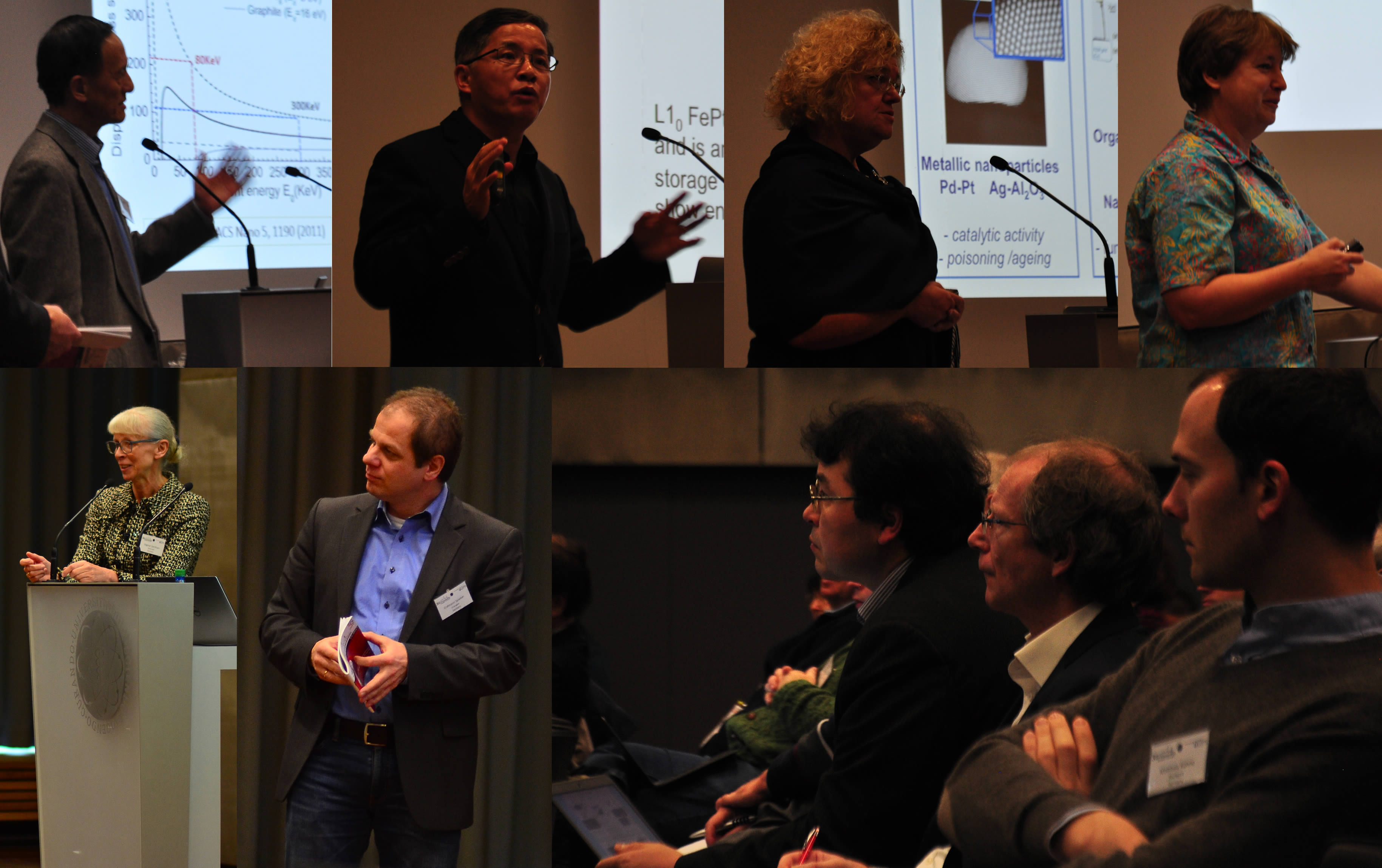
Figure 9: Session Techniques 1.
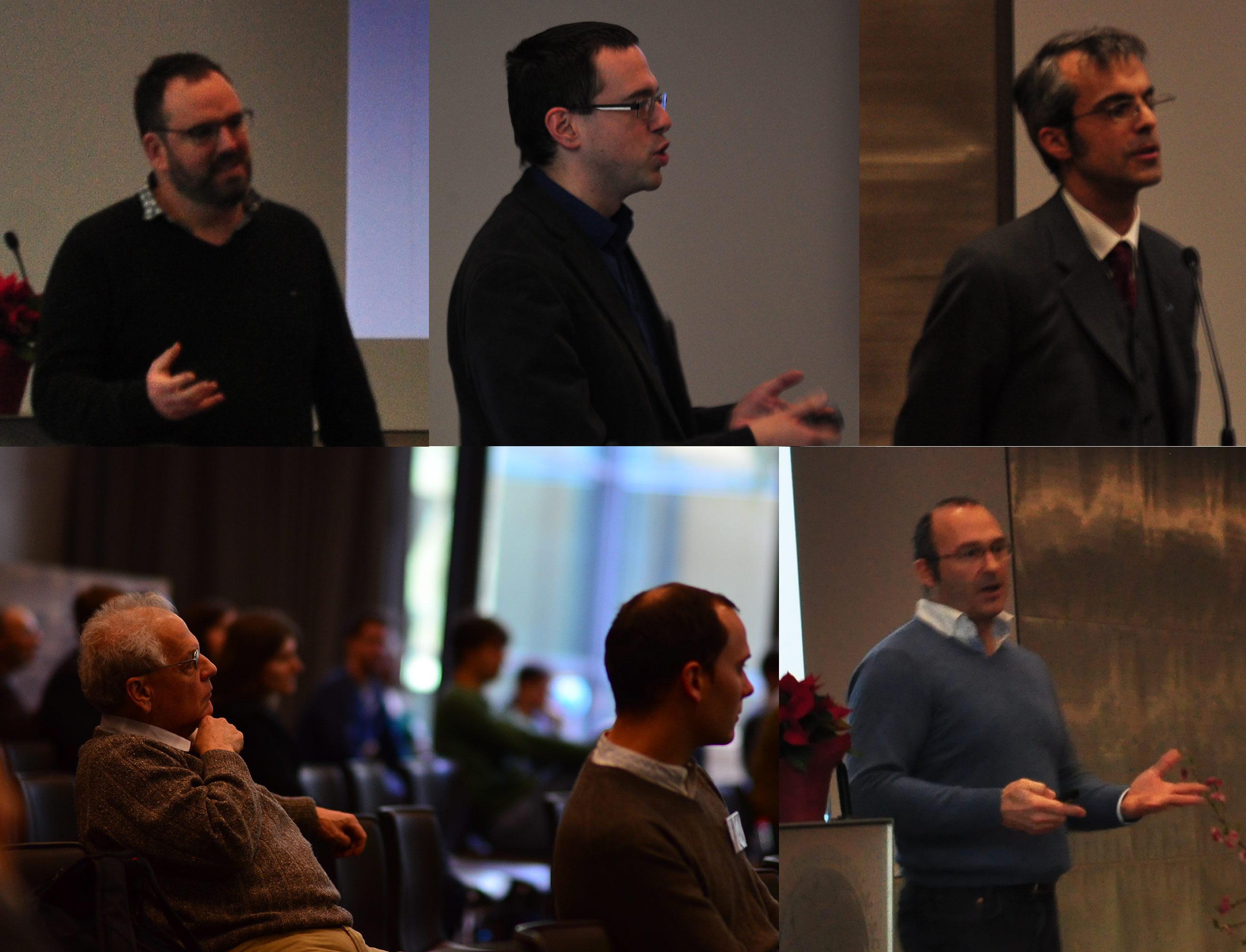
Figure 10: Session Techniques 2.
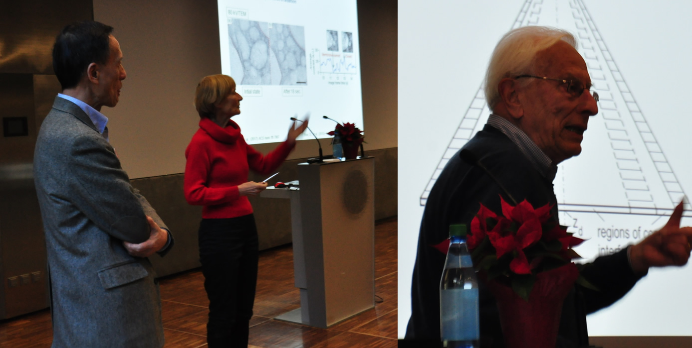
Figure 11: Session Techniques 3.
Sessions 4 “Advanced Techniques (I-III)”, chaired by Erdmann Spiecker, Christoph Koch, and Yimei Zhu
Recent advanced techniques for low-voltage electron microscopy have been presented in this session and it has been discussed to what extent the potential of the different technologies is already used in LV-AC-TEM and where improvements should be made.
Jianwei (John) Miao (University of California, US) has presented recent advances in atomic electron tomography (AET) on the example of grain boundaries, stacking faults and the 3D core structure of dislocations at atomic resolution. He showed that a 3D precision of 19 pm can be achieved in crystalline materials. He discussed recent experiments of AET of the 3D atomic positions of low-dimensional materials and proposed an outlook to 3D imaging of non-crystalline materials. Yimei Zhu (BNL, USA) presented latest state of the art results on in-situ electrochemical reaction for Li battery research and discussed the complexity of such a TEM study. Frances Ross (IBM, USA) applied environmental TEM (ETEM) on the understanding of epitaxial growth on graphene and discussed the opportunities for combining low keV imaging with ETEM capabilities to enhance our ability to extract growth physics during nanoscale materials reactions. Marc Willinger (FHI Berlin, Germany) showed that direct STEM-imaging of metal catalyzed chemical vapor deposition (CVD) of graphene is possible.
Lothar Houben (Weizmann Institute, Israel) reported on the experience they have gained with the chromatic aberration-corrected PICO instrument and compared to simulations. The practical applied chromatic aberration correction is only available since a very limited time. They have demonstrated latest experimental data on the effect of the chromatic aberration correction in EFTEM imaging. Among the benefits are fast two-dimensional mapping with wide field of view and atomic resolution and chemical composition mapping on the atomic scale under the constraint of the preservation of elastic contrast, which can be of advantage for e.g. recognition of dopants in capsule catalyst molecules. Dagmar Gerthsen (KIT, Germany) has shown a technique using transmission electron diffraction, SEM and STEM in parallel. It provides structural information, which cannot be seen using any of the techniques alone.
Tatiana Latychevskaia (Uni Zürich, Switzerland) showed a technique, namely low-energy (30 – 250 eV) electron in-line holography, which has delivered groundbreaking results in the last years. While it has been shown previously, that radiation damage in biological molecules is occuring at 3-20 eV, it was demonstrated that DNA can be imaged undestructively at energies such as 60, 115, and 230 eV. She reviewed these results and encouraged that the imaging of a biological molecule like DNA with atomic resolution will be possible in the future. She also showed again very significant progress in imaging if a charge of an impurity in graphene with this technique. Mathieu Kociak (CNRS/University Paris XI) reported on new technologies, which were recently explored in Belgium and France. They analyzed the STEM-EELS of nanoparticles and ions created in nanooptics. With their demonstration of the Purcell effect and the effect of symmetry breaking they expand the capabilities of TEM in the analysis of plasmons.
The potential of the differential phase contrast (DPC) method, in particular the annular differential phase contrast (ADPC) method was as already in the talk of Nobuo Tanaka also the topic of a second talk by Harald Rose (University Ulm, Germany). He showed on the example of focal series simulation, how the ADPC depth resolution improved in the last years with the correction of C3 and later C5 of the spherical aberration and the chromatic aberration and how the depth resolution would further improve with the complete elimination of Johnson noise in the future. The calculations were made for ADPC-STEM at an accelerating voltage of 30 kV, where a depth resolution of 0.3 nm could be achieved.
Similar to Harald Rose, Stefan Löffler (TU Vienna, Austria) reported on a further advancement of TEM that can be expected in the coming years. With the advancement in energy and spatial resolution, chemical mapping could become so sensitive, that the signal of individual orbitals can be isolated. It was shown in 2013 theoretically and recently in a proof-of-principle experiment that this technique, which is called “orbital mapping technique” is technically feasible. The key challenges to achieve this technique are (1) high point group symmetry of the scattering objects, (2) high signal/noise ratio, (3) stable Cs correction to high orders, and (4) Cc correction.
The topic of the talk by Ute Kaiser (University Ulm, Germany) was low-voltage aberration-corrected TEM (LV-AC-TEM) in general. She reviewed the transformation of this young technique since the beginning of the SALVE project. The reduction of the acceleration voltage had already been discussed in detail since 1970, mainly by Otto Scherzer for TEM and by Albert Crewe for STEM as possibly very fruitful. The materials under investigation they had in mind already included the most sensitive: biological materials. Since first realization of a spherical aberration-corrected instrument operating at 80 kV in 2005 by the companies FEI and CEOS GmbH is today regarded as the starting point of LV-AC-TEM. And indeed the pioneers were correct in their assessment of the potential of this technique. Although already this technique has produced a rather large number of publications with high scientific impact, it still needs to be shown and this is one near-future task, how far we can go in imaging single molecules in high resolution.
The topic of the talk by Ute Kaiser (University Ulm, Germany) was low-voltage aberration-corrected TEM (LV-AC-TEM) in general. She reviewed the transformation of this young technique since the beginning of the SALVE project. The reduction of the acceleration voltage had already been discussed in detail since 1970, mainly by Otto Scherzer for TEM and by Albert Crewe for STEM as possibly very fruitful. The materials under investigation they had in mind already included the most sensitive: biological materials. Since first realization of a spherical aberration-corrected instrument operating at 80 kV in 2005 by the companies FEI and CEOS GmbH is today regarded as the starting point of LV-AC-TEM. And indeed the pioneers were correct in their assessment of the potential of this technique. Although already this technique has produced a rather large number of publications with high scientific impact, it still needs to be shown and this is one near-future task, how far we can go in imaging single molecules in high resolution.
Apart from the lectures, the importance of scientific discussions during the coffee-breaks, dinners and other social activities (visit of the Ulm cathedral with organ music, late-night piano concert in the city hall with Valerij Petasch) must be underlined. The direct contact stimulated the exchange of ideas and establishing of new co-operations and friendship.
Finally, the organization of the events would not be possible without generous financial support of the public institutions and international organizations – the University of Ulm, the German Research Foundation (DFG), the manufactures Thermo Fisher Scientific, CEOS GmbH, Gatan, JEOL, and the German Society of Electron Microscopy – DGE.